SNOSDC3D June 2021 – July 2022 TLV3601-Q1 , TLV3602-Q1 , TLV3603-Q1
PRODMIX
- 1 Features
- 2 Applications
- 3 Description
- 4 Revision History
- 5 Pin Configuration and Functions
- 6 Specifications
- 7 Detailed Description
- 8 Application and Implementation
- 9 Power Supply Recommendations
- 10Layout
- 11Device and Documentation Support
- 12Mechanical, Packaging, and Orderable Information
Package Options
Mechanical Data (Package|Pins)
Thermal pad, mechanical data (Package|Pins)
Orderable Information
5 Pin Configuration and Functions
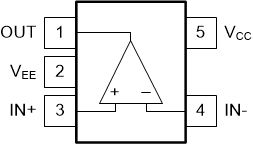
 Figure 5-1 DCK, DBV Package
5-Pin SC70, SOT-23
Top View
Figure 5-2 DCK Package
6-Pin SC70
Top View
6-Pin SC70
Top View
Table 5-1 Pin
Functions
| PIN | I/O | DESCRIPTION | ||
|---|---|---|---|---|
| NAME | TLV3601 | TLV3603 | ||
| IN+ | 3 | 3 | I | Non-inverting input |
| IN– | 4 | 4 | I | Inverting input |
| OUT | 1 | 1 | O | Output (Push-pull) |
| VEE | 2 | 2 | I | Negative power supply |
| VCC | 5 | 6 | I | Positive power supply |
| LE/HYS | - | 5 | I | Adjustable hysteresis control and latch |
Figure 5-3 TLV3602 DGK, DSG Packages
8-Pin VSSOP, WSON
8-Pin VSSOP, WSON
Table 5-2 Pin Functions: TLV3602
(Dual)
| PIN | I/O | DESCRIPTION | |
|---|---|---|---|
| NAME | NO. | ||
| IN1+ |
1 |
I | Noninverting input, channel 1 |
| IN1– |
2 |
I | Inverting input, channel 1 |
| IN2– |
3 |
I | Inverting input, channel 2 |
| IN2+ |
4 |
I | Noninverting input, channel 2 |
| OUT1 |
7 |
O | Output, channel 1 |
| OUT2 |
6 |
O | Output, channel 2 |
| V- |
5 |
P | Negative (lowest) supply or ground |
| V+ | 8 | P | Positive (highest) supply |
| Thermal PAD | - | Connect directly to V- pin | |