SNOSDB1E june 2021 – april 2023 TLV3601 , TLV3602 , TLV3603 , TLV3603E
PRODUCTION DATA
- 1 Features
- 2 Applications
- 3 Description
- 4 Revision History
- 5 Pin Configuration and Functions
- 6 Specifications
- 7 Detailed Description
- 8 Application and Implementation
- 9 Power Supply Recommendations
- 10Layout
- 11Device and Documentation Support
- 12Mechanical, Packaging, and Orderable Information
Package Options
Mechanical Data (Package|Pins)
- DCK|6
Thermal pad, mechanical data (Package|Pins)
Orderable Information
8.1.3 Latch Functionality
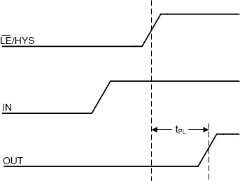
The latch pin for the TLV3603(E) holds the output state of the device when the voltage at the LE/HYS pin is a logic low. This is particularly useful when the output state is intended to remain unchanged. An important consideration of the latch functionality is the latch hold and setup times. Latch hold time is the minimum time required (after the latch pin is asserted) for properly latching the comparator output. Likewise, latch setup time is defined as the time that the input must be stable before the latch pin is asserted low. The figure below illustrates when the input can transition for a valid latch. Note that the typical setup time in the EC table is negative; this is due to the internal trace delays of the LE/HYS pin relative to the input pin trace delays. A small delay (tPL) in the output response is shown below when the TLV3603(E) exits a latched output stage.
 Figure 8-3 Input Change Properly Latched
 Figure 8-4 Latch Disable with Input Change