SNOSDA2F August   2020  – June 2024 TLV3604 , TLV3605 , TLV3607

PRODUCTION DATA  

  1.   1
  2. Features
  3. Applications
  4. Description
  5. Pin Configuration and Functions
    1.     Pin Configurations: TLV3604 and TLV3605
    2. 4.1 Pin Configuration: TLV3607
  6. Specifications
    1. 5.1 Absolute Maximum Ratings
    2. 5.2 ESD Ratings
    3. 5.3 Recommended Operating Conditions
    4. 5.4 Thermal Information
    5. 5.5 Electrical Characteristics (VCCI = VCCO = 2.5V to 5V)
    6. 5.6 Typical Characteristics
  7. Detailed Description
    1. 6.1 Overview
    2. 6.2 Functional Block Diagram
    3. 6.3 Feature Description
    4. 6.4 Device Functional Modes
      1. 6.4.1 Rail-to-Rail Inputs
      2. 6.4.2 LVDS Output
  8. Application and Implementation
    1. 7.1 Application Information
      1. 7.1.1 Comparator Inputs
      2. 7.1.2 Capacitive Loads
      3. 7.1.3 Latch Functionality
      4. 7.1.4 Adjustable Hysteresis
    2. 7.2 Typical Application
      1. 7.2.1 Non-Inverting Comparator With Hysteresis
        1. 7.2.1.1 Design Requirements
        2. 7.2.1.2 Detailed Design Procedure
        3. 7.2.1.3 Application Performance Plots
      2. 7.2.2 Optical Receiver
      3. 7.2.3 Logic Clock Source to LVDS Transceiver
      4. 7.2.4 External Trigger Function for Oscilloscopes
    3. 7.3 Power Supply Recommendations
    4. 7.4 Layout
      1. 7.4.1 Layout Guidelines
      2. 7.4.2 Layout Example
  9. Device and Documentation Support
    1. 8.1 Device Support
      1. 8.1.1 Development Support
    2. 8.2 Receiving Notification of Documentation Updates
    3. 8.3 Support Resources
    4. 8.4 Trademarks
    5. 8.5 Electrostatic Discharge Caution
    6. 8.6 Glossary
  10. Revision History
  11. 10Mechanical, Packaging, and Orderable Information

Package Options

Mechanical Data (Package|Pins)
Thermal pad, mechanical data (Package|Pins)
Orderable Information

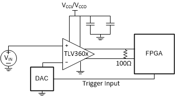
External Trigger Function for Oscilloscopes

Figure 7-9 is a typical configuration for creating an external trigger on oscilliscopes. The user adjusts the trigger level, and a DAC converts this trigger level to a voltage the TLV360x can use as a reference. The input voltage from an oscilloscope channel is then compared to the trigger reference voltage, and the TLV3604, TLV3605, and TLV3607 sends an LVDS signal to a downstream FPGA to begin a capture.
TLV3604 TLV3605 TLV3607 External Trigger FunctionFigure 7-9 External Trigger Function