SNOSDA2F August 2020 – June 2024 TLV3604 , TLV3605 , TLV3607
PRODUCTION DATA
- 1
- 1 Features
- 2 Applications
- 3 Description
- 4 Pin Configuration and Functions
- 5 Specifications
- 6 Detailed Description
- 7 Application and Implementation
- 8 Device and Documentation Support
- 9 Revision History
- 10Mechanical, Packaging, and Orderable Information
Package Options
Mechanical Data (Package|Pins)
- DCK|6
Thermal pad, mechanical data (Package|Pins)
Orderable Information
7.1.4 Adjustable Hysteresis
As a result of a comparator’s high open loop gain, there is a small band of input differential voltage where the output can toggle back and forth between “logic high” and “logic low” states. This can cause design challenges for inputs with slow rise and fall times or systems with excessive noise.
These challenges can be overcome by adding hysteresis to the comparator. Since the TLV3604 does not have internal hysteresis, external hysteresis can be applied in the form of a positive feedback loop that adjusts the trip point of the comparator depending on its current output state. See the Typical Application section for more details.
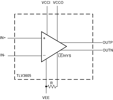
The TLV3605 and TLV3607 have a LEB/HYST pin that can be used to increase the internal hysteresis of the comparator. To change the internal hysteresis of the TLV3605 and TLV3607, connect a single resistor as shown in the adjusting hysteresis figure between the LEB/HYST pin and VEE. A curve of hysteresis versus resistance is provided below to provide guidance in setting the desired amount of hysteresis.
 Figure 7-3 Adjusting Hysteresis with an External Resistor (R)
 Figure 7-4 VHYST (mV) vs RHYST (kΩ), VCC = 3.3V