SNOSDA2F August   2020  – June 2024 TLV3604 , TLV3605 , TLV3607

PRODUCTION DATA  

  1.   1
  2. Features
  3. Applications
  4. Description
  5. Pin Configuration and Functions
    1.     Pin Configurations: TLV3604 and TLV3605
    2. 4.1 Pin Configuration: TLV3607
  6. Specifications
    1. 5.1 Absolute Maximum Ratings
    2. 5.2 ESD Ratings
    3. 5.3 Recommended Operating Conditions
    4. 5.4 Thermal Information
    5. 5.5 Electrical Characteristics (VCCI = VCCO = 2.5V to 5V)
    6. 5.6 Typical Characteristics
  7. Detailed Description
    1. 6.1 Overview
    2. 6.2 Functional Block Diagram
    3. 6.3 Feature Description
    4. 6.4 Device Functional Modes
      1. 6.4.1 Rail-to-Rail Inputs
      2. 6.4.2 LVDS Output
  8. Application and Implementation
    1. 7.1 Application Information
      1. 7.1.1 Comparator Inputs
      2. 7.1.2 Capacitive Loads
      3. 7.1.3 Latch Functionality
      4. 7.1.4 Adjustable Hysteresis
    2. 7.2 Typical Application
      1. 7.2.1 Non-Inverting Comparator With Hysteresis
        1. 7.2.1.1 Design Requirements
        2. 7.2.1.2 Detailed Design Procedure
        3. 7.2.1.3 Application Performance Plots
      2. 7.2.2 Optical Receiver
      3. 7.2.3 Logic Clock Source to LVDS Transceiver
      4. 7.2.4 External Trigger Function for Oscilloscopes
    3. 7.3 Power Supply Recommendations
    4. 7.4 Layout
      1. 7.4.1 Layout Guidelines
      2. 7.4.2 Layout Example
  9. Device and Documentation Support
    1. 8.1 Device Support
      1. 8.1.1 Development Support
    2. 8.2 Receiving Notification of Documentation Updates
    3. 8.3 Support Resources
    4. 8.4 Trademarks
    5. 8.5 Electrostatic Discharge Caution
    6. 8.6 Glossary
  10. Revision History
  11. 10Mechanical, Packaging, and Orderable Information

Package Options

Mechanical Data (Package|Pins)
Thermal pad, mechanical data (Package|Pins)
Orderable Information

Pin Configurations: TLV3604 and TLV3605
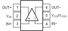
TLV3604 TLV3605 TLV3607 DCK Package6-Pin SC70Top ViewFigure 4-1 DCK Package
6-Pin SC70
Top View
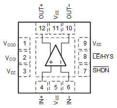
TLV3604 TLV3605 TLV3607 RVK Package12-Pin QFNTop ViewFigure 4-2 RVK Package
12-Pin QFN
Top View
Table 4-1 Pin Functions: TLV3604 and TLV3605
PINI/ODESCRIPTION
NAMETLV3604TLV3605
IN+34INon-inverting input
IN–46IInverting input
OUT+112ONon-inverting output
OUT–610OInverting output
VEE23, 5, 9, 11INegative power supply
VCCI52IPositive input section power supply
VCCO51IPositive output section power supply
SHDN-7IShutdown control, active low
LE/HYS-8IAdjustable hysteresis control and latch