SBOSAA8C December 2022 – August 2024 TLV2365 , TLV365
PRODUCTION DATA
- 1
- 1 Features
- 2 Applications
- 3 Description
- 4 Device Comparison Table
- 5 Pin Configuration and Functions
- 6 Specifications
- 7 Detailed Description
- 8 Application and Implementation
- 9 Device and Documentation Support
- 10Revision History
- 11Mechanical, Packaging, and Orderable Information
Package Options
Refer to the PDF data sheet for device specific package drawings
Mechanical Data (Package|Pins)
- DBV|5
Thermal pad, mechanical data (Package|Pins)
Orderable Information
7.3.4 Active Filter
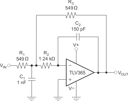
The TLVx365 is an excellent choice for active filter applications requiring a wide bandwidth, fast slew rate, low-noise, single-supply operational amplifier. Figure 7-6 shows a 500-kHz, second-order, low-pass filter using a multiple-feedback (MFB) topology. The components have been selected to provide a maximally-flat Butterworth response. Beyond the cutoff frequency, rolloff is −40 dB/dec. The Butterworth response is designed for applications requiring predictable gain characteristics, such as the antialiasing filter used ahead of an ADC.
 Figure 7-6 Second-Order Butterworth, 500-kHz Low-Pass Filter
When considering the MFB filter, the output is inverted, relative to the input. If this inversion is not desired, then a noninverting output can be achieved through one of these options:
- add an inverting amplifier
- add an additional second-order MFB stage
- use a noninverting filter topology, such as the Sallen-Key
Figure 7-7 shows the Sallen-Key topology.
 Figure 7-7 Configured as a Three-Pole, 20-kHz, Sallen-Key Filter