SNVSBU0 October   2020 TLV4062-Q1 , TLV4082-Q1

PRODUCTION DATA  

  1. Features
  2. Applications
  3. Description
  4. Revision History
  5. Pin Configuration and Functions
  6. Specifications
    1. 6.1 Absolute Maximum Ratings
    2. 6.2 ESD Ratings
    3. 6.3 Recommended Operating Conditions
    4. 6.4 Thermal Information
    5. 6.5 Electrical Characteristics
    6. 6.6 Timing Requirements
    7. 6.7 Timing Diagrams
    8. 6.8 Typical Characteristics
  7. Detailed Description
    1. 7.1 Overview
    2. 7.2 Functional Block Diagrams
    3. 7.3 Feature Description
    4. 7.4 Device Functional Modes
      1. 7.4.1 Inputs (IN1, IN2)
      2. 7.4.2 Outputs (OUT1, OUT2)
      3. 7.4.3 Switching Threshold and Hysteresis
  8. Application and Implementation
    1. 8.1 Application Information
      1. 8.1.1 Threshold Overdrive
    2. 8.2 Typical Applications
      1. 8.2.1 Monitoring Two Separate Rails
        1. 8.2.1.1 Design Requirements
        2. 8.2.1.2 Detailed Design Procedure
        3. 8.2.1.3 Application Curve
      2. 8.2.2 Early Warning Detection
        1. 8.2.2.1 Design Requirements
        2. 8.2.2.2 Detailed Design Procedure
        3. 8.2.2.3 Application Curve
      3. 8.2.3 Additional Application Information
        1. 8.2.3.1 Pull-Up Resistor Selection
        2. 8.2.3.2 INx Capacitor
  9. Power Supply Recommendations
  10. 10Layout
    1. 10.1 Layout Guidelines
    2. 10.2 Layout Example
  11. 11Device and Documentation Support
    1. 11.1 Documentation Support
      1. 11.1.1 Related Documentation
    2. 11.2 Receiving Notification of Documentation Updates
    3. 11.3 Support Resources
    4. 11.4 Trademarks
    5. 11.5 Electrostatic Discharge Caution
    6. 11.6 Glossary

Package Options

Mechanical Data (Package|Pins)
Thermal pad, mechanical data (Package|Pins)
Orderable Information

Typical Characteristics

at TJ = 25°C with a 0.1-µF capacitor close to V+ (unless otherwise noted)
GUID-825F1D81-E967-4A2C-A4D7-12DC31A3D2DE-low.gif
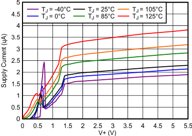
IN1 = IN2 = 1.5 V
Figure 6-2 Supply Current vs Supply Voltage
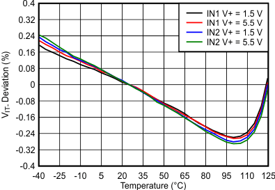
GUID-F55DD948-BB80-44FB-9933-7160B2A37278-low.gifFigure 6-4 INx Threshold (VIT–) Deviation vs Temperature
GUID-E8E76B09-A896-496A-BF54-AF04242E77DD-low.gif
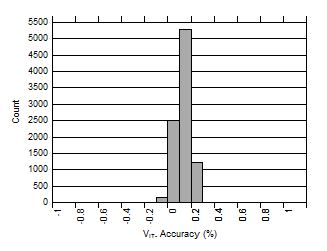
V+ = 5.5 V
Figure 6-6 INx Threshold (VIT–)
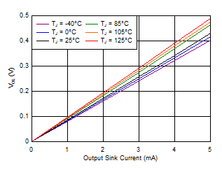
GUID-A26C40A6-82F5-463C-B8E4-5D9735C2F53D-low.gifFigure 6-8 Output Voltage Low vs Output Current (V+ = 3.3 V)
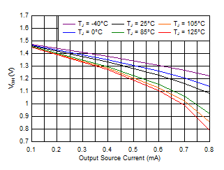
GUID-15F8121F-30A7-4384-9D3C-502C6A22C06F-low.gifFigure 6-10 Output Voltage High vs Output Current (V+ = 1.5 V)
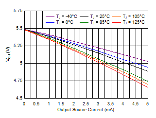
GUID-42086255-9DE7-43B1-AE13-7F79356D1491-low.gifFigure 6-12 Output Voltage High vs Output Current (V+ = 5.5 V)
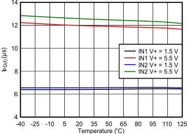
GUID-9A54B6F5-07C5-4B77-BD8A-D58A3230A3C6-low.gif
IN1 = IN2 = 1.3 V to 0 V
Figure 6-14 Propagation Delay from INx Low to Output Low
GUID-10EED823-6631-4541-BC34-132D415E9A9E-low.gif
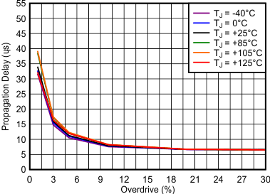
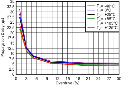
High-to-low transition occurs above the curve
Figure 6-16 Propagation Delay vs Overdrive (V+ = 1.5 V)
GUID-72E7FC92-2B14-43D9-A4F8-F919C3A5556C-low.gif
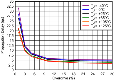
Low-to-high transition occurs above the curve
Figure 6-18 Propagation Delay vs Overdrive (V+ = 1.5 V)
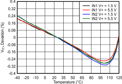
GUID-8471532D-D94A-4845-B91B-62FDA59E4313-low.gifFigure 6-3 INx Threshold (VIT+) Deviation vs Temperature
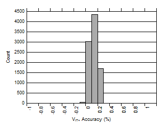
GUID-20F17969-2859-4E76-A6EE-0123E13341C2-low.gif
V+ = 5.5 V
Figure 6-5 INx Threshold (VIT+)
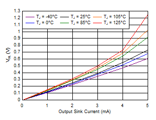
GUID-391788CF-2691-4D35-98FF-B9868331041C-low.gifFigure 6-7 Output Voltage Low vs Output Current (V+ = 1.5 V)
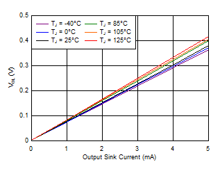
GUID-4F496BFF-96F9-4B55-94AA-3047A79A7A0A-low.gifFigure 6-9 Output Voltage Low vs Output Current (V+ = 5.5 V)
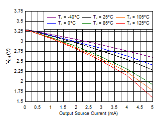
GUID-1D4D63ED-1AB4-48EB-AAFA-B2061FFB0362-low.gifFigure 6-11 Output Voltage High vs Output Current (V+ = 3.3 V)
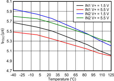
GUID-355E6AF5-2FD4-4279-8037-A5006C436A81-low.gif
IN1 = IN2 = 0 V to 1.3 V
Figure 6-13 Propagation Delay from INx High to Output High
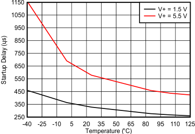
GUID-EC1DE091-76AB-4AC2-9F9F-65DDA3B5ACE4-low.gifFigure 6-15 Startup Delay
GUID-B01DC609-925F-409E-8157-97DDFCB3BF8D-low.gif
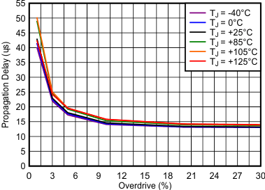
High-to-low transition occurs above the curve
Figure 6-17 Propagation Delay vs Overdrive (V+ = 5.5 V)
GUID-0055DDE5-567F-42D1-BE34-E9ABB928A9D9-low.gif
Low-to-high transition occurs above the curve
Figure 6-19 Propagation Delay vs Overdrive (V+ = 5.5 V)