SNOSD27 May 2016 TLV522
PRODUCTION DATA.
- 1 Features
- 2 Applications
- 3 Description
- 4 Revision History
- 5 Pin Configuration and Functions
- 6 Specifications
- 7 Detailed Description
- 8 Application and Implementation
- 9 Power Supply Recommendations
- 10Layout
- 11Device and Documentation Support
- 12Mechanical, Packaging, and Orderable Information
Package Options
Mechanical Data (Package|Pins)
- DGK|8
Thermal pad, mechanical data (Package|Pins)
Orderable Information
8 Application and Implementation
NOTE
Information in the following applications sections is not part of the TI component specification, and TI does not warrant its accuracy or completeness. TI’s customers are responsible for determining suitability of components for their purposes. Customers should validate and test their design implementation to confirm system functionality.
8.1 Application Information
The TLV522 is a ultra-low power operational amplifier that provides 8 kHz bandwidth with only 490 nA quiescent current, and near precision offset and drift specifications at a low cost. These rail-to-rail input and output amplifiers are specifically designed for battery-powered applications. The input common-mode voltage range extends to the power-supply rails and the output swings to within millivolts of the rails, maintaining a wide dynamic range.
8.2 Typical Application: 60 Hz Twin "T" Notch Filter
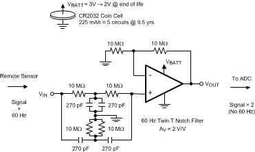
 Figure 24. 60 Hz Notch Filter
8.2.1 Design Requirements
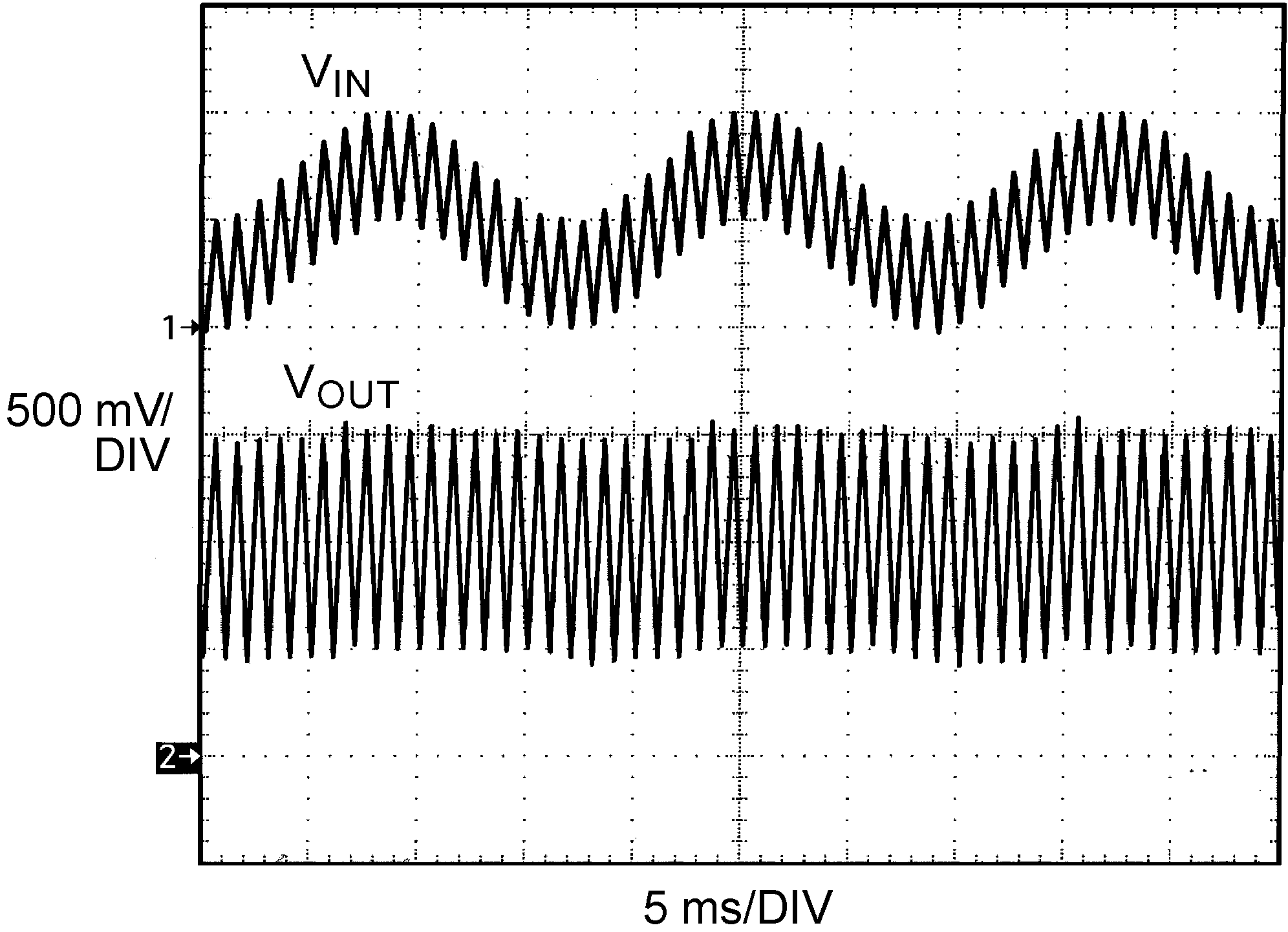
Small signals from transducers in remote and distributed sensing applications commonly suffer strong 60 Hz interference from AC power lines. The circuit of Figure 24 notches out the 60 Hz and provides a gain AV = 2 for the sensor signal represented by a 1 kHz sine wave. Similar stages may be cascaded to remove 2nd and 3rd harmonics of 60 Hz. Thanks to the nA power consumption of the TLV522, even 5 such circuits can run for 9.5 years from a small CR2032 lithium cell. These batteries have a nominal voltage of 3 V and an end of life voltage of 2 V. With an operating voltage from 1.7 V to 5.5 V the TLV522 can function over this voltage range.
8.2.2 Detailed Design Procedure
The notch frequency is set by:
To achieve a 60 Hz notch use R = 10 MΩ and C = 270 pF. If eliminating 50 Hz noise, which is common in European systems, use R = 11.8 MΩ and C = 270 pF.
The Twin T Notch Filter works by having two separate paths from VIN to the amplifier’s input. A low frequency path through the series input resistors and another separate high frequency path through the series input capacitors. However, at frequencies around the notch frequency, the two paths have opposing phase angles and the two signals will tend to cancel at the amplifier’s input.
To ensure that the target center frequency is achieved and to maximize the notch depth (Q factor) the filter needs to be as balanced as possible. To obtain circuit balance, while overcoming limitations of available standard resistor and capacitor values, use passives in parallel to achieve the 2C and R/2 circuit requirements for the filter components that connect to ground.
To make sure passive component values stay as expected clean board with alcohol, rinse with deionized water, and air dry. Make sure board remains in a relatively low humidity environment to minimize moisture which may increase the conductivity of board components. Also large resistors come with considerable parasitic stray capacitance which effects can be reduced by cutting out the ground plane below components of concern.
Large resistors are used in the feedback network to minimize battery drain. When designing with large resistors, resistor thermal noise, op amp current noise, as well as op amp voltage noise, must be considered in the noise analysis of the circuit. The noise analysis for the circuit in Figure 24 can be done over a bandwidth of 2 kHz, which takes the conservative approach of overestimating the bandwidth (TLV522 typical GBW/AV is lower). The total noise at the output is approximately 800 µVpp, which is excellent considering the total consumption of the circuit is only 900 nA. The dominant noise terms are op amp voltage noise , current noise through the feedback network (430 µVpp), and current noise through the notch filter network (280 µVpp). Thus the total circuit's noise is below 1/2 LSB of a 10-bit system with a 2 V reference, which is 1 mV.
8.2.3 Application Curve
 Figure 25. 60 Hz Notch Filter Waveform
8.3 Do's and Don'ts
Do properly bypass the power supplies.
Do add series resistance to the output when driving capacitive loads, particularly cables, MUX and ADC inputs.
Do add series current limiting resistors and external schottky clamp diodes if input voltage is expected to exceed the supplies. Limit the current to 1 mA or less (1 KΩ per volt).