SLVSD82B April 2017 – February 2021 TLV61046A
PRODUCTION DATA
- 1 Features
- 2 Applications
- 3 Description
- 4 Revision History
- 5 Pin Configuration and Functions
- 6 Specifications
- 7 Detailed Description
- 8 Application and Implementation
- 9 Power Supply Recommendations
- 10Layout
- 11Device and Documentation Support
- 12Mechanical, Packaging, and Orderable Information
Package Options
Mechanical Data (Package|Pins)
- DBV|6
Thermal pad, mechanical data (Package|Pins)
Orderable Information
8.2.2.4 Input and Output Capacitor Selection
The output capacitor is mainly selected to meet the requirements for output ripple and loop stability. This ripple voltage is related to the capacitance of the capacitor and its equivalent series resistance (ESR). Assuming a ceramic capacitor with zero ESR, the minimum capacitance needed for a given ripple can be calculated by:
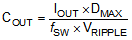
where
- DMAX is maximum switching duty cycle
- VRIPPLE is peak to peak output voltage ripple
The ESR impact on the output ripple must be considered if tantalum or aluminum electrolytic capacitors are used.
Care must be taken when evaluating a ceramic capacitor’s derating under dc bias, aging, and ac signal. For example, the dc bias can significantly reduce capacitance. A ceramic capacitor can lose more than 50% of its capacitance at its rated voltage. Therefore, always leave margin on the voltage rating to ensure adequate capacitance at the required output voltage.
It is recommended to use the output capacitor with effective capacitance in the range of 0.47 μF to 10 μF. The output capacitor affects loop stability of the boost regulator. If the output capacitor is below the range, the boost regulator can potentially become unstable. Increasing the output capacitor makes the output voltage ripple smaller in PWM mode.
For input capacitor, a ceramic capacitor with more than 1.0 µF is enough for most applications.