SLVSEX0A March   2019  – July 2019 TLV61048

PRODUCTION DATA.  

  1. Features
  2. Applications
  3. Description
    1.     Device Images
      1.      Simplified Schematic
  4. Revision History
  5. Pin Configuration and Functions
    1.     Pin Functions
  6. Specifications
    1. 6.1 Absolute Maximum Ratings
    2. 6.2 ESD Ratings
    3. 6.3 Recommended Operating Conditions
    4. 6.4 Thermal Information
    5. 6.5 Electrical Characteristics
    6. 6.6 Typical Characteristics
  7. Detailed Description
    1. 7.1 Overview
    2. 7.2 Functional Block Diagram
    3. 7.3 Feature Description
      1. 7.3.1 Undervoltage Lockout
      2. 7.3.2 Enable and Disable
      3. 7.3.3 Soft Start
      4. 7.3.4 Frequency Select (FREQ)
    4. 7.4 Device Functional Modes
      1. 7.4.1 PWM Mode
      2. 7.4.2 PFM Mode
  8. Application and Implementation
    1. 8.1 Application Information
    2. 8.2 Typical Applications
      1. 8.2.1 12-V Output Boost Converter With External Bias
        1. 8.2.1.1 Design Requirements
        2. 8.2.1.2 Detailed Design Procedure
          1. 8.2.1.2.1 Programming the Output Voltage
          2. 8.2.1.2.2 Inductor Selection
          3. 8.2.1.2.3 Input and Output Capacitor Selection
          4. 8.2.1.2.4 Diode Rectifier Selection
        3. 8.2.1.3 Application Curves
      2. 8.2.2 14-V Output Boost Converter
        1. 8.2.2.1 Design Requirements
        2. 8.2.2.2 Detailed Design Procedure
          1. 8.2.2.2.1 Inductor Selection
          2. 8.2.2.2.2 Input and Output Capacitor Selection
  9. Power Supply Recommendations
  10. 10Layout
    1. 10.1 Layout Guidelines
    2. 10.2 Layout Example
  11. 11Device and Documentation Support
    1. 11.1 Device Support
      1. 11.1.1 Third-Party Products Disclaimer
    2. 11.2 Receiving Notification of Documentation Updates
    3. 11.3 Community Resources
    4. 11.4 Trademarks
    5. 11.5 Electrostatic Discharge Caution
    6. 11.6 Glossary
  12. 12Mechanical, Packaging, and Orderable Information

Package Options

Mechanical Data (Package|Pins)
Thermal pad, mechanical data (Package|Pins)
Orderable Information

Pin Configuration and Functions

DBV Package
6-Pin SOT-23
Top View
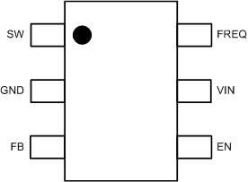
TLV61048 pinout_SLVSEX0.gif

Pin Functions

PIN I/O DESCRIPTION
NO. NAME
1 SW PWR The switch pin of the converter. It is connected to the drain of the internal power MOSFET.
2 GND PWR Ground
3 FB I Voltage feedback of output voltage. Connected to the center tap of a resistor divider to program the output voltage.
4 EN I Enable logic input. Logic high voltage enables the device. Logic low voltage disables the device and turns it into shutdown mode.
5 VIN I IC power supply input
6 FREQ I Frequency select pin. The device operates at 600 kHz if FREQ is left floating or pulled high and at 1 MHz if connected to GND.