SLVSBB9F March 2012 – January 2017 TLV62090
PRODUCTION DATA.
- 1 Features
- 2 Applications
- 3 Description
- 4 Revision History
- 5 Pin Configuration and Functions
- 6 Specifications
- 7 Detailed Description
- 8 Application and Implementation
- 9 Power Supply Recommendations
- 10Layout
- 11Device and Documentation Support
- 12Mechanical, Packaging, and Orderable Information
Package Options
Refer to the PDF data sheet for device specific package drawings
Mechanical Data (Package|Pins)
- RGT|16
Thermal pad, mechanical data (Package|Pins)
Orderable Information
7 Detailed Description
7.1 Overview
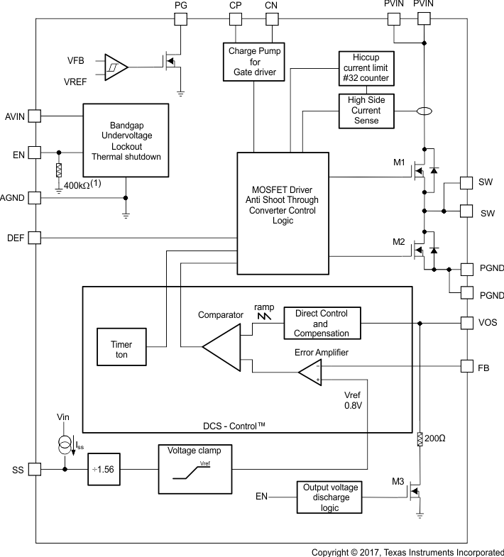
The TLV62090 synchronous switched mode converter is based on DCS-Control™ (direct control with seamless transition into power save mode). This is an advanced regulation topology that combines the advantages of hysteretic and voltage-mode control.
The DCS-Control™ topology operates in pulse width modulation (PWM) mode for medium to heavy load conditions and in power save mode at light load currents. In PWM mode, the converter operates with its nominal switching frequency of 1.4 MHz having a controlled frequency variation over the input voltage range. As the load current decreases, the converter enters power save mode, reducing the switching frequency and minimizing the current consumption to achieve high efficiency over the entire load current range. DCS-Control™ supports both operation modes (PWM and PFM) using a single building block having a seamless transition from PWM to power save mode without effects on the output voltage. The TLV62090 offers excellent DC voltage regulation and load transient regulation, combined with low output voltage ripple, minimizing interference with RF circuits.
7.3 Feature Description
7.3.1 Enable (EN)
The device is enabled by setting the EN pin to a logic high. Accordingly, shutdown mode is forced if the EN pin is pulled low with a shutdown current of typically 0.6 µA. In shutdown mode, the internal power switches as well as the entire control circuitry are turned off. An internal resistor of 200 Ω discharges the output through the VOS pin smoothly. An internal pull-down resistor of 400 kΩ is connected to the EN pin when the EN pin is low. The pull-down resistor is disconnected when the EN pin is high.
7.3.2 Softstart (SS) and Hiccup Current Limit During Startup
To minimize inrush current during start up, the device has an adjustable softstart depending on the capacitor value connected to the SS pin. The device charges the softstart capacitor with a constant current of typically 7.5 µA. The feedback voltage follows this voltage with a fraction of 1.56 until the internal reference voltage of 0.8 V is reached. Softstart operation is completed once the voltage at the softstart capacitor has reached typically 1.25 V. The softstart time is calculated using Equation 1. The larger the softstart capacitor, the longer the softstart time. The relation between softstart voltage and feedback voltage is estimated using Equation 2.


During startup, the switch current limit is reduced to 1/3 (~1.5 A) of its typical current limit of 4.6 A. Once the output voltage exceeds typically 0.6 V, the current limit is released to its nominal value. The device provides a reduced load current of ~1.5 A when the output voltage is below typically 0.6 V. Due to this, a small or no softstart time may trigger the short circuit protection during startup especially for larger output capacitors. This is avoided by using a larger softstart capacitance to extend the softstart time. See Short Circuit Protection (Hiccup-Mode) for details of the reduced current limit during startup. Leaving the softstart pin floating sets the minimum startup time (around 50 µs).
7.3.3 Voltage Tracking (SS)
The SS pin is externally driven by another voltage source to achieve output voltage tracking. The application circuit is shown in Figure 9. The internal reference voltage follows the voltage at the SS pin with a fraction of 1.56 until the internal reference voltage of 0.8 V is reached. The device achieves ratiometric or coincidental (simultaneous) output tracking, as shown in Figure 10.
The R2 value should be set properly to achieve accurate voltage tracking by taking 7.5 μA soft startup current into account. 1 kΩ or smaller is a sufficient value for R2.
For decreasing the SS pin voltage, the device doesn't sink current from the output when the device is in power save mode. So the resulting decreases of the output voltage may be slower than the SS pin voltage if the load is light. When driving the SS pin with an external voltage, do not exceed the voltage rating of the SS pin which is
7 V.
7.3.4 Short Circuit Protection (Hiccup-Mode)
The device is protected against hard short circuits to GND and over-current events. This is implemented by a two level short circuit protection. During startup and when the output is shorted to GND, the switch current limit is reduced to 1/3 of its typical current limit of 4.6 A. Once the output voltage exceeds typically 0.6 V, the current limit is released to its nominal value. The full current limit is implemented as a hiccup current limit. Once the internal current limit is triggered 32 times, the device stops switching and starts a new startup sequence after a typical delay time of 66 µS. The device goes through these cycles until the high current condition is released.
7.3.5 Output Discharge Function
To make sure the device starts up under defined conditions, the output gets discharged via the VOS pin with a typical discharge resistor of 200 Ω whenever the device shuts down. This happens when the device is disabled or if thermal shutdown, undervoltage lockout or short circuit hiccup-mode are triggered.
7.3.6 Power Good Output (PG)
The power good output is low when the output voltage is below its nominal value. The power good becomes high impedance once the output is within 5% of regulation. The PG pin is an open drain output and is specified to typically sink up to 1 mA. This output requires a pull-up resistor to be monitored properly. The pull-up resistor cannot be connected to any voltage higher than the input voltage of the device. The PG output is low when the device is disabled, in thermal shutdown or UVLO. The PG output can be left floating if unused. Table 1 shows the PG pin logic.
7.3.7 Undervoltage Lockout (UVLO)
To avoid mis-operation of the device at low input voltages, an undervoltage lockout is included. UVLO shuts down the device at input voltages lower than typically 2.2 V with a 200 mV hysteresis.
7.3.8 Thermal Shutdown
The device goes into thermal shutdown once the junction temperature exceeds typically 150°C with a 20°C hysteresis.
7.3.9 Charge Pump (CP, CN)
The CP and CN pins must attach to an external 10 nF capacitor to complete a charge pump for the gate driver. This capacitor must be rated for the input voltage. It is not recommended to connect any other circuits to the CP or CN pins.
7.4 Device Functional Modes
7.4.1 PWM Operation
At medium to heavy load currents, the device operates with pulse width modulation (PWM) at a nominal switching frequency of 1.4 MHz. As the load current decreases, the converter enters power save mode operation reducing its switching frequency. The device enters power save mode at the boundary to discontinuous conduction mode (DCM).
7.4.2 Power Save Mode Operation
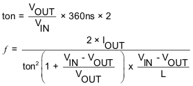
As the load current decreases, the converter enters power save mode operation. During power save mode, the converter operates with reduced switching frequency maintaining high efficiency. Power save mode is based on a fixed on-time architecture following Equation 3.

In power save mode, the output voltage rises slightly above the nominal output voltage in PWM mode, as shown in Figure 15. This effect is reduced by increasing the output capacitance or the inductor value. This effect is also reduced by programming the output voltage of the TLV62090 lower than the target value. As an example, if the target output voltage is 3.3 V, then the TLV62090 can be programmed to 3.3 V - 0.8%. As a result the output voltage accuracy is now -2.2% to +2.2% instead of -1.4% to 3%. The output voltage accuracy in pulse frequency modulation (PFM) operation is reflected in the electrical specification table and given for a 22-µF output capacitor.
7.4.3 Low Dropout Operation (100% Duty Cycle)
The device offers a low input to output voltage difference by entering 100% duty cycle mode. In this mode, the high-side MOSFET switch is constantly turned on. This is particularly useful in battery powered applications to achieve longest operation time by taking full advantage of the whole battery voltage range. The minimum input voltage where the output voltage falls below its nominal regulation value is given by:
Where
RDS(on) = High side FET on-resistance
RL = DC resistance of the inductor
