SLVSBB9F March   2012  – January 2017 TLV62090

PRODUCTION DATA.  

  1. Features
  2. Applications
  3. Description
  4. Revision History
  5. Pin Configuration and Functions
  6. Specifications
    1. 6.1 Absolute Maximum Ratings
    2. 6.2 ESD Ratings
    3. 6.3 Recommended Operating Conditions
    4. 6.4 Thermal Information
    5. 6.5 Electrical Characteristics
    6. 6.6 Typical Characteristics
  7. Detailed Description
    1. 7.1 Overview
    2. 7.2 Functional Block Diagram
    3. 7.3 Feature Description
      1. 7.3.1 Enable (EN)
      2. 7.3.2 Softstart (SS) and Hiccup Current Limit During Startup
      3. 7.3.3 Voltage Tracking (SS)
      4. 7.3.4 Short Circuit Protection (Hiccup-Mode)
      5. 7.3.5 Output Discharge Function
      6. 7.3.6 Power Good Output (PG)
      7. 7.3.7 Undervoltage Lockout (UVLO)
      8. 7.3.8 Thermal Shutdown
      9. 7.3.9 Charge Pump (CP, CN)
    4. 7.4 Device Functional Modes
      1. 7.4.1 PWM Operation
      2. 7.4.2 Power Save Mode Operation
      3. 7.4.3 Low Dropout Operation (100% Duty Cycle)
  8. Application and Implementation
    1. 8.1 Application Information
    2. 8.2 Typical Application
      1. 8.2.1 Design Requirements
      2. 8.2.2 Detailed Design Procedure
        1. 8.2.2.1 Custom Design with WEBENCH® Tools
        2. 8.2.2.2 Inductor Selection
        3. 8.2.2.3 Input and Output Capacitor Selection
        4. 8.2.2.4 Setting the Output Voltage
      3. 8.2.3 Application Curves
  9. Power Supply Recommendations
  10. 10Layout
    1. 10.1 Layout Guideline
    2. 10.2 Layout Example
  11. 11Device and Documentation Support
    1. 11.1 Device Support
      1. 11.1.1 Custom Design with WEBENCH® Tools
    2. 11.2 Documentation Support
      1. 11.2.1 Third-Party Products Disclaimer
    3. 11.3 Receiving Notification of Documentation Updates
    4. 11.4 Community Resources
    5. 11.5 Trademarks
    6. 11.6 Electrostatic Discharge Caution
    7. 11.7 Glossary
  12. 12Mechanical, Packaging, and Orderable Information

Package Options

Refer to the PDF data sheet for device specific package drawings

Mechanical Data (Package|Pins)
  • RGT|16
Thermal pad, mechanical data (Package|Pins)
Orderable Information

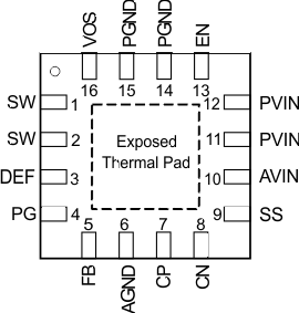
Pin Configuration and Functions

RGT Package
16-Pin VQFN
Top View
TLV62090 po_lvsbb9.gif

Pin Functions

PIN I/O DESCRIPTION
NAME NO.
SW 1, 2 I/O Switch pin of the power stage.
DEF 3 I This pin is used for internal logic and needs to be pulled high. This pin should not be left floating.
PG 4 O Power good open drain output. This pin is high impedance if the output voltage is within regulation. This pin is pulled low if the output is below its nominal value. The pull up resistor can not be connected to any voltage higher than the input voltage of the device.
FB 5 I Feedback pin of the device. Connect a resistor divider to set the output voltage.
AGND 6 Analog ground.
CP 7 I/O Internal charge pump flying capacitor. Connect a 10 nF capacitor between CP and CN.
CN 8 I/O Internal charge pump flying capacitor. Connect a 10 nF capacitor between CP and CN.
SS 9 I Softstart control pin. A capacitor is connected to this pin and sets the softstart time. Leaving this pin floating sets the minimum start-up time.
AVIN 10 I Bias supply input voltage pin.
PVIN 11,12 I Power supply input voltage pin.
EN 13 I Device enable. To enable the device this pin needs to be pulled high. Pulling this pin low disables the device. This pin has a pull down resistor of typically 400 kΩ, which is active when EN is low.
PGND 14,15 Power ground connection.
VOS 16 I Output voltage sense pin. This pin needs to be connected to the output voltage.
Exposed Thermal Pad The exposed thermal pad is connected to AGND. It must be soldered for mechanical reliability.