SLVSDG1C DECEMBER 2016 – October 2017 TLV62569
UNLESS OTHERWISE NOTED, this document contains PRODUCTION DATA.
- 1 Features
- 2 Applications
- 3 Description
- 4 Revision History
- 5 Pin Configuration and Functions
- 6 Specifications
- 7 Detailed Description
- 8 Application and Implementation
- 9 Power Supply Recommendations
- 10Layout
- 11Device and Documentation Support
- 12Mechanical, Packaging, and Orderable Information
Package Options
Mechanical Data (Package|Pins)
Thermal pad, mechanical data (Package|Pins)
Orderable Information
8 Application and Implementation
NOTE
Information in the following applications sections is not part of the TI component specification, and TI does not warrant its accuracy or completeness. TI’s customers are responsible for determining suitability of components for their purposes. Customers should validate and test their design implementation to confirm system functionality.
8.1 Application Information
The following section discusses the design of the external components to complete the power supply design for several input and output voltage options by using typical applications as a reference.
8.2 Typical Application
 Figure 5. TLV62569 1.8-V Output Application
8.2.1 Design Requirements
For this design example, use the parameters listed in Table 2 as the input parameters.
Table 2. Design Parameters
| DESIGN PARAMETER | EXAMPLE VALUE |
|---|---|
| Input voltage | 2.5 V to 5.5 V |
| Output voltage | 1.8 V |
| Maximum output current | 2.0 A |
Table 3 lists the components used for the example.
Table 3. List of Components
| REFERENCE | DESCRIPTION | MANUFACTURER(1) |
|---|---|---|
| C1 | 4.7 µF, Ceramic Capacitor, 10 V, X7R, size 0805, GRM21BR71A475KA73L | Murata |
| C2 | 10 µF, Ceramic Capacitor, 10 V, X7R, size 0805, GRM21BR71A106KE51L | Murata |
| L1 | 2.2 µH, Power Inductor, size 4mmx4mm, XAL4020-222ME | Coilcraft |
| R1,R2,R3 | Chip resistor,1%,size 0603 | Std. |
| C3 | Optional, 6.8 pF if it is needed | Std. |
8.2.2 Detailed Design Procedure
8.2.2.1 Custom Design With WEBENCH® Tools
Click here to create a custom design using the TLV62569 device with the WEBENCH® Power Designer.
- Start by entering the input voltage (VIN), output voltage (VOUT), and output current (IOUT) requirements.
- Optimize the design for key parameters such as efficiency, footprint, and cost using the optimizer dial.
- Compare the generated design with other possible solutions from Texas Instruments.
The WEBENCH Power Designer provides a customized schematic along with a list of materials with real-time pricing and component availability.
In most cases, these actions are available:
- Run electrical simulations to see important waveforms and circuit performance
- Run thermal simulations to understand board thermal performance
- Export customized schematic and layout into popular CAD formats
- Print PDF reports for the design, and share the design with colleagues
Get more information about WEBENCH tools at www.ti.com/WEBENCH.
8.2.2.2 Setting the Output Voltage
An external resistor divider is used to set output voltage according to Equation 2.
When sizing R2, in order to achieve low current consumption and acceptable noise sensitivity, use a maximum of 200 kΩ for R2. Larger currents through R2 improve noise sensitivity and output voltage accuracy but increase current consumption.

A feed forward capacitor, C3 improves the loop bandwidth to make a fast transient response (shown in Figure 19). 6.8-pF capacitance is recommended for R2 of 100-kΩ resistance. A more detailed discussion on the optimization for stability vs. transient response can be found in SLVA289.
8.2.2.3 Output Filter Design
The inductor and output capacitor together provide a low-pass filter. To simplify this process, Table 4 outlines possible inductor and capacitor value combinations. Checked cells represent combinations that are proven for stability by simulation and lab test. Further combinations should be checked for each individual application.
Table 4. Matrix of Output Capacitor and Inductor Combinations
| VOUT [V] | L [µH](1) | COUT [µF](2) | ||||
|---|---|---|---|---|---|---|
| 4.7 | 10 | 22 | 2 x 22 | 100 | ||
| 0.6 ≤ VOUT < 1.2 | 1 | + | ||||
| 2.2 | ++(3) | |||||
| 1.2 ≤ VOUT < 1.8 | 1 | + | + | |||
| 2.2 | ++(3) | + | ||||
| 1.8 ≤ VOUT | 1 | + | + | + | ||
| 2.2 | ++(3) | + | + | |||
8.2.2.4 Inductor Selection
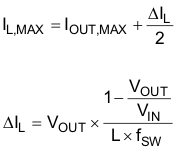
The main parameters for inductor selection is inductor value and then saturation current of the inductor. To calculate the maximum inductor current under static load conditions, Equation 3 is given:

where
- IOUT,MAX is the maximum output current
- ΔIL is the inductor current ripple
- fSW is the switching frequency
- L is the inductor value
It is recommended to choose a saturation current for the inductor that is approximately 20% to 30% higher than IL,MAX. In addition, DC resistance and size should also be taken into account when selecting an appropriate inductor.
8.2.2.5 Input and Output Capacitor Selection
The architecture of the TLV62569 allows use of tiny ceramic-type output capacitors with low equivalent series resistance (ESR). These capacitors provide low output voltage ripple and are thus recommended. To keep its resistance up to high frequencies and to achieve narrow capacitance variation with temperature, it is recommended to use X7R or X5R dielectric.
The input capacitor is the low impedance energy source for the converter that helps provide stable operation. A low ESR multilayer ceramic capacitor is recommended for best filtering. For most applications, 4.7-μF input capacitance is sufficient; a larger value reduces input voltage ripple.
The TLV62569 is designed to operate with an output capacitor of 10 µF to 47 µF, as outlined in Table 4.
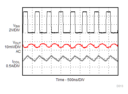
8.2.3 Application Performance Curves
VIN = 5 V, VOUT = 1.8 V, L = 2.2 μH, TA = 25 °C, unless otherwise noted.


| VIN = 5 V |

| VIN = 5 V |

| IOUT = 1 A |

| IOUT = 2 A |

| Load Step 0.8 A to 2 A, 1A/μs slew rate | ||

| VOUT = 1.8 V |

| IOUT = 1 A |

| IOUT = 0.1 A |

| IOUT = 0.1 A |

| Load Step 0.8 A to 2 A, 1A/μs slew rate | C3 = 6.8 pF | |