SLUSDR2A December   2020  – January 2023 TLV62595

PRODUCTION DATA  

  1. Features
  2. Applications
  3. Description
  4. Revision History
  5. Pin Configuration and Functions
  6. Specifications
    1. 6.1 Absolute Maximum Ratings
    2. 6.2 ESD Ratings
    3. 6.3 Recommended Operating Conditions
    4. 6.4 Thermal Information
    5. 6.5 Electrical Characteristics
    6. 6.6 Typical Characteristics
  7. Detailed Description
    1. 7.1 Overview
    2. 7.2 Functional Block Diagram
    3. 7.3 Feature Description
      1. 7.3.1 Pulse Width Modulation (PWM) Operation
      2. 7.3.2 Power Save Mode (PSM) Operation
      3. 7.3.3 Minimum Duty Cycle and 100% Mode Operation
      4. 7.3.4 Soft Start
      5. 7.3.5 Switch Current Limit and HICCUP Short-Circuit Protection
      6. 7.3.6 Undervoltage Lockout
      7. 7.3.7 Thermal Shutdown
    4. 7.4 Device Functional Modes
      1. 7.4.1 Enable, Disable and Output Discharge
      2. 7.4.2 Power Good
  8. Application and Implementation
    1. 8.1 Application Information
    2. 8.2 Typical Application
      1. 8.2.1 Design Requirements
      2. 8.2.2 Detailed Design Procedure
        1. 8.2.2.1 Custom Design With WEBENCH® Tools
        2. 8.2.2.2 Setting The Output Voltage
        3. 8.2.2.3 Output Filter Design
        4. 8.2.2.4 Inductor Selection
        5. 8.2.2.5 Capacitor Selection
      3. 8.2.3 Application Curves
    3. 8.3 Power Supply Recommendations
    4. 8.4 Layout
      1. 8.4.1 Layout Guidelines
      2. 8.4.2 Layout Example
        1. 8.4.2.1 Thermal Considerations
  9. Device and Documentation Support
    1. 9.1 Device Support
      1. 9.1.1 Third-Party Products Disclaimer
      2. 9.1.2 Development Support
        1. 9.1.2.1 Custom Design With WEBENCH® Tools
    2. 9.2 Documentation Support
      1. 9.2.1 Related Documentation
    3. 9.3 Receiving Notification of Documentation Updates
    4. 9.4 Support Resources
    5. 9.5 Trademarks
    6. 9.6 Electrostatic Discharge Caution
    7. 9.7 Glossary
  10. 10Mechanical, Packaging, and Orderable Information

Package Options

Mechanical Data (Package|Pins)
Thermal pad, mechanical data (Package|Pins)
Orderable Information

Application Curves

VIN = 5.0 V, VOUT = 1.8 V, TA = 25°C, BOM = Table 8-2, unless otherwise noted.
VIN = 5.0 V, VOUT = 1.8 V, TA = 25°C, BOM = Table 8-2, unless otherwise noted.GUID-A5262459-C723-4203-B817-6F4E27B170AD-low.gif
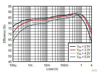
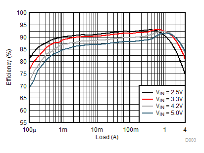
VOUT = 0.6 V
Figure 8-2 Efficiency. VIN = 5.0 V, VOUT = 1.8 V, TA = 25°C, BOM = Table 8-2, unless otherwise noted.
GUID-2962B9B3-F8A6-465C-984A-6DEA85D7108A-low.gif
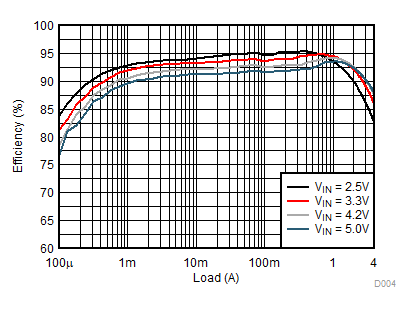
VOUT = 1.2 V
Figure 8-4 Efficiency
GUID-18382729-9F82-48C8-833E-45EB64D324FD-low.gif
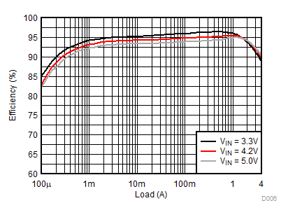
VOUT = 1.8 V
Figure 8-6 Efficiency
GUID-3E505F03-0508-4E8C-ADDF-FD49B57B37E5-low.gif
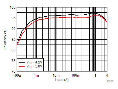
VOUT = 2.5 V
Figure 8-8 Efficiency
GUID-A9AAD678-6EB3-4ABA-B3C7-9D4FC3E54317-low.gif
VOUT = 3.3 V
Figure 8-10 Efficiency
GUID-E3AB4F4A-2F93-4B7F-9B13-987F4D54809C-low.gif
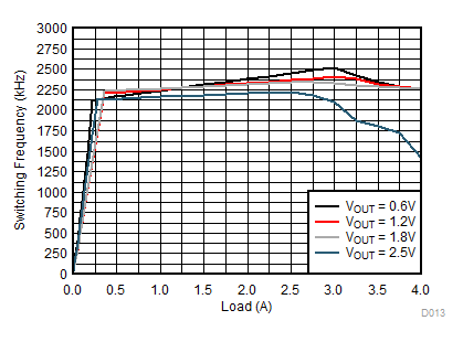
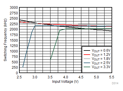
VIN = 3.3 V
Figure 8-12 Switching Frequency
GUID-218E8B07-072C-437F-B00C-71F8C9AB6757-low.gif
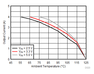
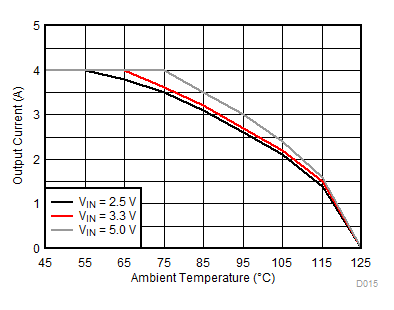
VOUT = 1.2 V θJA= 71.4 °C/W
Figure 8-14 Thermal Derating
GUID-EF95438C-CB89-4F5E-AA48-965F1763BAF1-low.gif
VOUT = 2.5 V θJA= 71.4 °C/W
Figure 8-16 Thermal Derating
GUID-288F28E3-BED6-474A-9D1E-C96193C48C38-low.gif
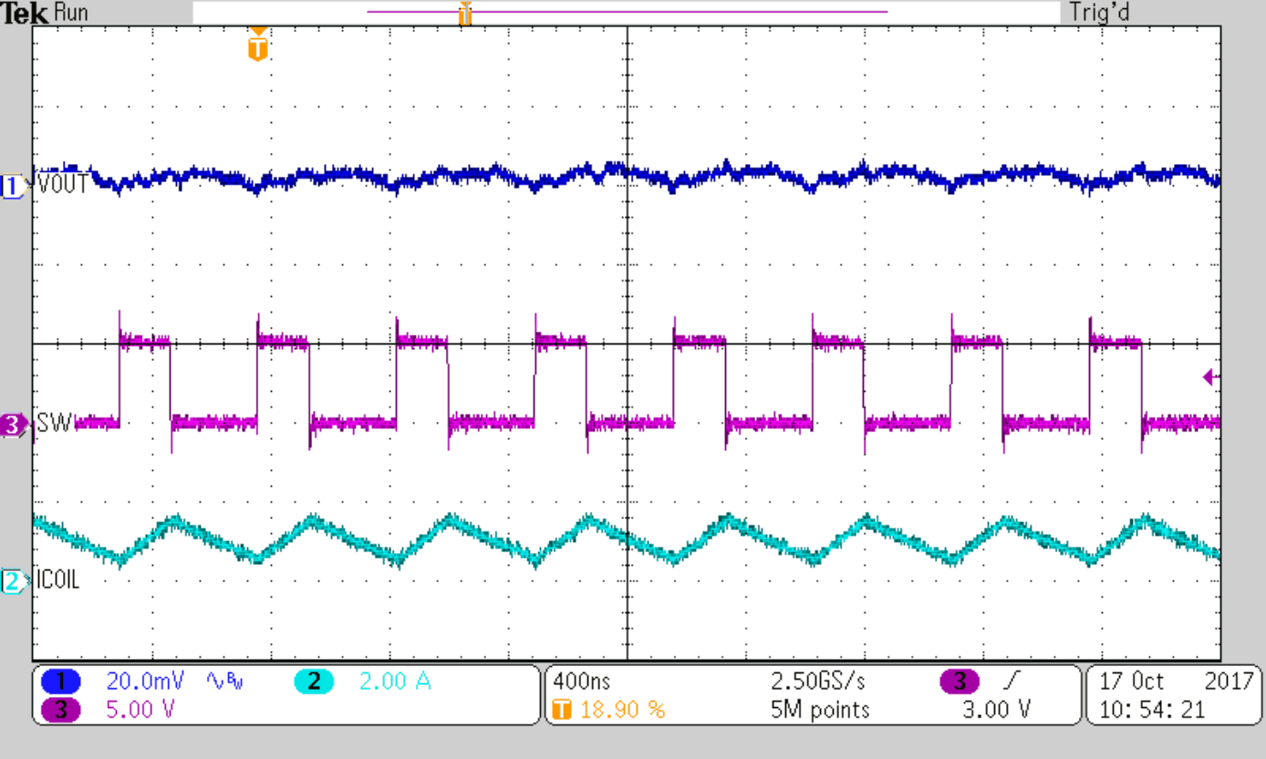
IOUT = 1.0 A
Figure 8-18 PWM Operation
GUID-F58770CB-E531-4D0E-960F-7FA8633ED7F3-low.gif
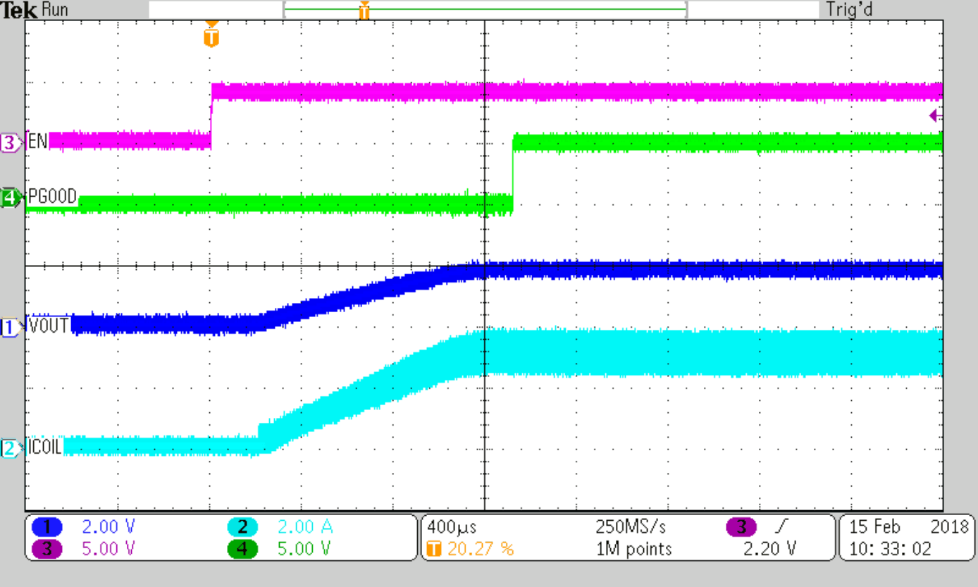
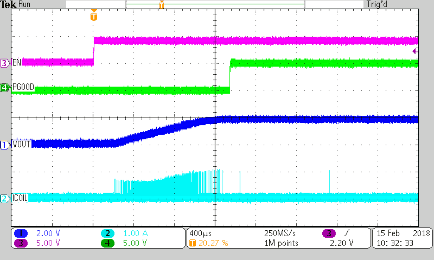
Load = 0.6 Ω
Figure 8-20 Start-up with Load
GUID-55CF06F1-B6AF-4B62-9201-1641095605DC-low.gif
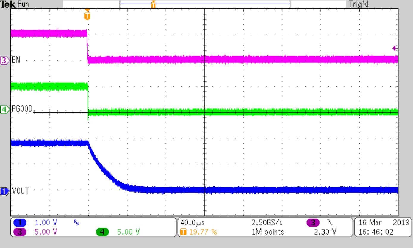
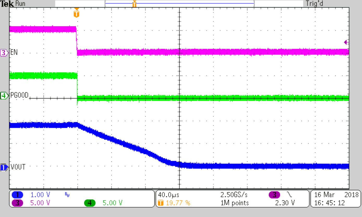
Load = 1.8 Ω
Figure 8-22 Disable, Active Output Discharge
GUID-374A6018-D78C-4829-B853-26078AA0FE2F-low.gif
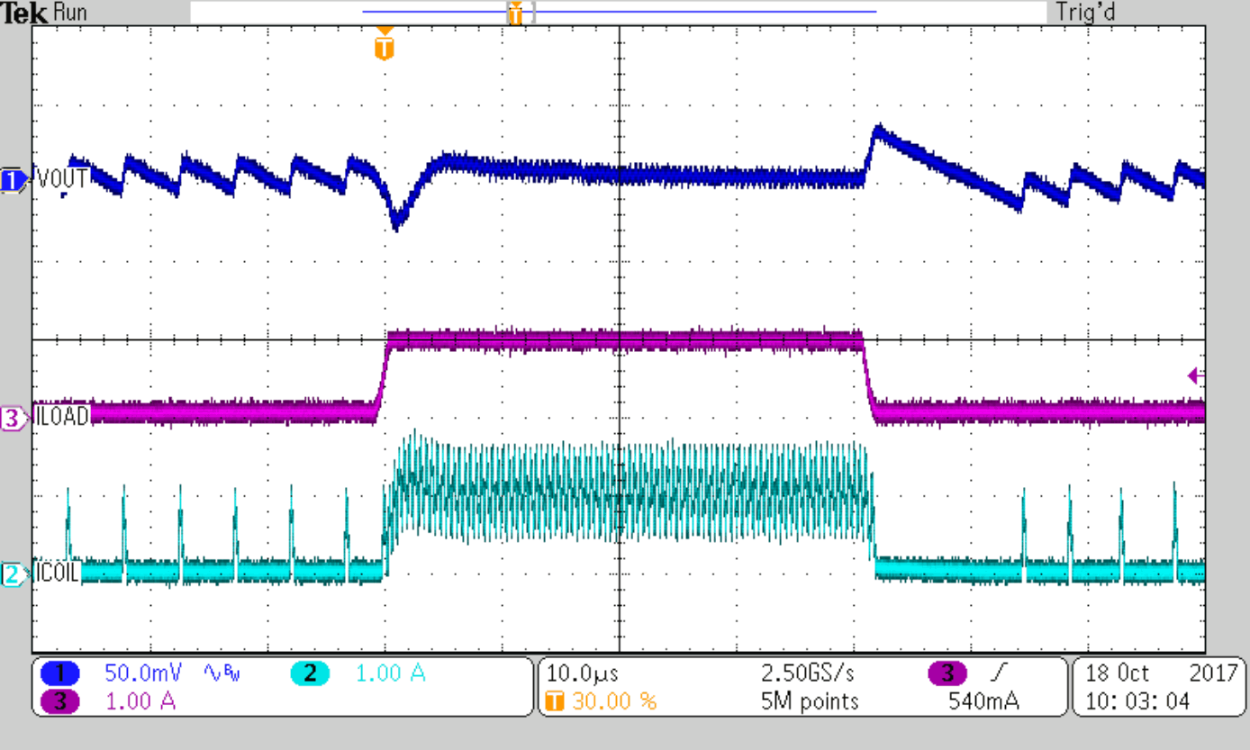
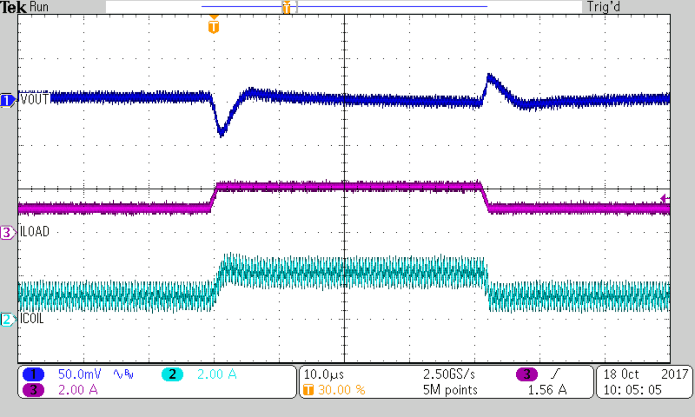
IOUT = 0.05 A to 1A
Figure 8-24 Load Transient
GUID-9A85FC9C-7064-426B-BA0D-255665EC0017-low.gif
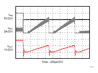
IOUT = 1 A
Figure 8-26 HICCUP Short Circuit Protection
GUID-F9E688C6-7366-4F62-9479-AF610EAD32A6-low.gif
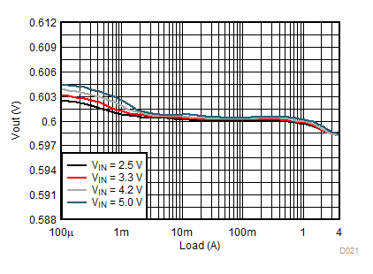
VOUT = 0.6 V
Figure 8-3 Load Regulation
GUID-1081B9F6-7B3C-4A2E-9930-150245DFD886-low.gif
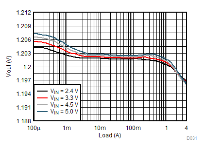
VOUT = 1.2 V
Figure 8-5 Load Regulation
GUID-CAE4190D-50A6-4AEB-AB26-5C352F754A02-low.gif
VOUT = 1.8 V
Figure 8-7 Load Regulation
GUID-B382DB33-F475-4812-9C86-C4C04FF97C0B-low.gif
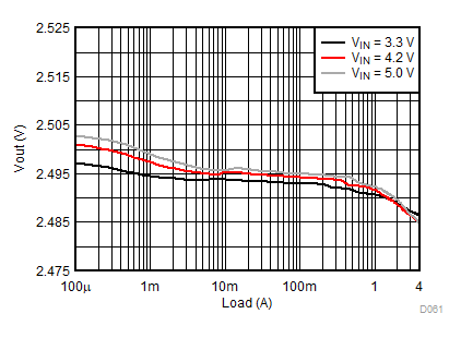
VOUT = 2.5 V
Figure 8-9 Load Regulation
GUID-C0B7C5A8-CB1A-47DB-8FA4-B053145F8B31-low.gif
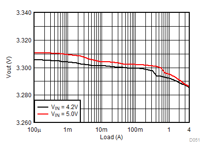
VOUT = 3.3 V
Figure 8-11 Load Regulation
GUID-2B344D5D-768E-4483-A67E-39D799356A05-low.gif
IOUT = 1.0 A
Figure 8-13 Switching Frequency
GUID-E2D213A4-FA01-45FC-8BC0-F7FBE62E44CE-low.gif
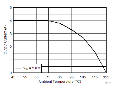
VOUT = 1.8 V θJA= 71.4 °C/W
Figure 8-15 Thermal Derating
GUID-DDD300C1-5227-48A0-B12E-2571ABBE0604-low.gif
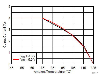
VOUT = 3.3 V θJA= 71.4 °C/W
Figure 8-17 Thermal Derating
GUID-7711387C-8BA9-452A-A71A-0B93D51D6709-low.gif
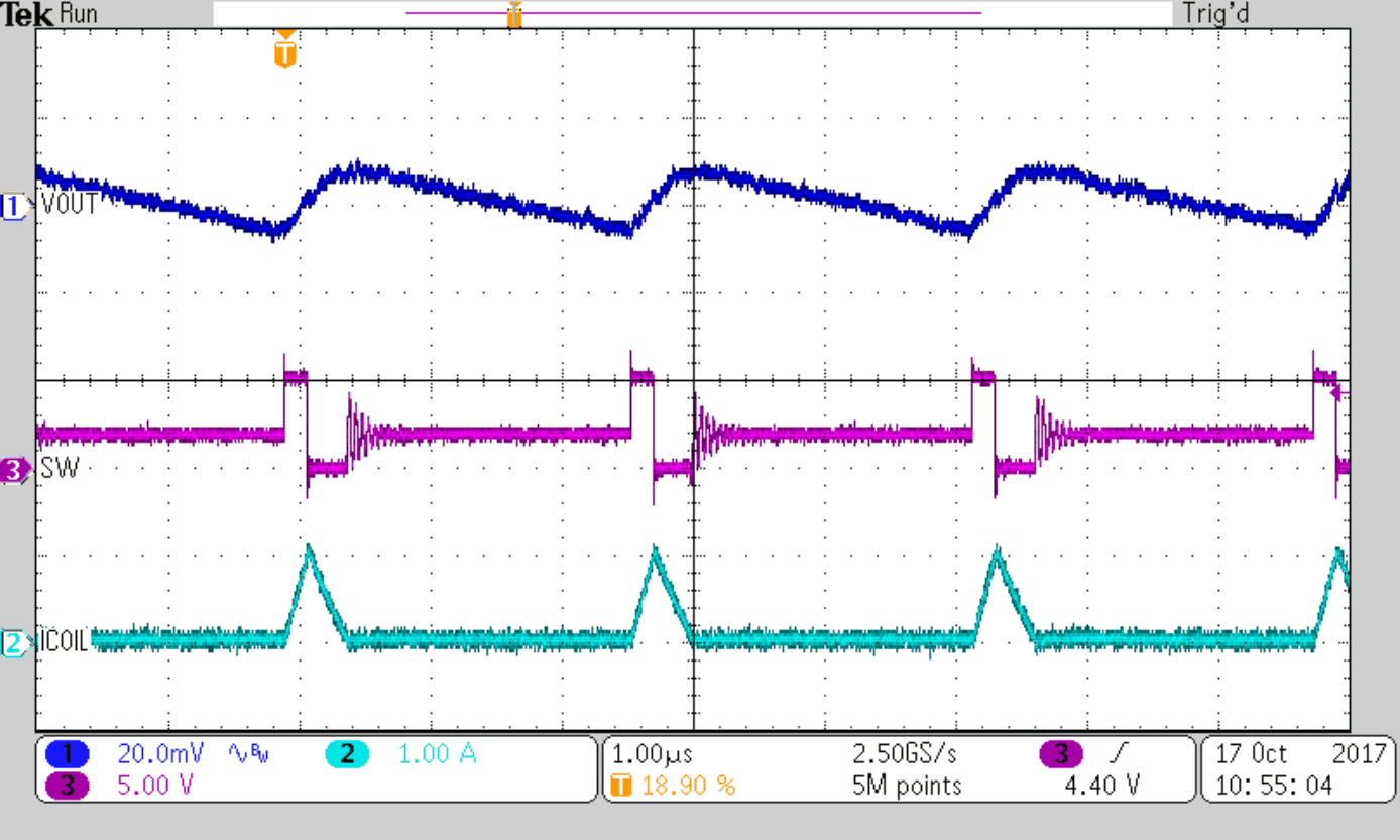
IOUT = 0.1 A
Figure 8-19 PSM Operation
GUID-18D5903F-80E4-496E-9375-91B5D227A719-low.gif
 
Figure 8-21 Startup with No Load
GUID-0254B80A-EBF9-4292-9929-70A9624F818D-low.gif
 
Figure 8-23 Disable, Active Output Discharge at No Load
GUID-EA490D81-C621-472D-8468-321EB95EF1E4-low.gif
IOUT = 1 A to 2 A
Figure 8-25 Load Transient
GUID-FB50DDDB-E920-46B9-9B27-7CEF6A9A5D72-low.gif
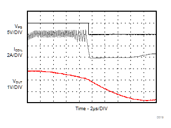
IOUT = 1 A
Figure 8-27 HICCUP Short Circuit Protection (Zoom In)