SLUSDR2A December   2020  – January 2023 TLV62595

PRODUCTION DATA  

  1. Features
  2. Applications
  3. Description
  4. Revision History
  5. Pin Configuration and Functions
  6. Specifications
    1. 6.1 Absolute Maximum Ratings
    2. 6.2 ESD Ratings
    3. 6.3 Recommended Operating Conditions
    4. 6.4 Thermal Information
    5. 6.5 Electrical Characteristics
    6. 6.6 Typical Characteristics
  7. Detailed Description
    1. 7.1 Overview
    2. 7.2 Functional Block Diagram
    3. 7.3 Feature Description
      1. 7.3.1 Pulse Width Modulation (PWM) Operation
      2. 7.3.2 Power Save Mode (PSM) Operation
      3. 7.3.3 Minimum Duty Cycle and 100% Mode Operation
      4. 7.3.4 Soft Start
      5. 7.3.5 Switch Current Limit and HICCUP Short-Circuit Protection
      6. 7.3.6 Undervoltage Lockout
      7. 7.3.7 Thermal Shutdown
    4. 7.4 Device Functional Modes
      1. 7.4.1 Enable, Disable and Output Discharge
      2. 7.4.2 Power Good
  8. Application and Implementation
    1. 8.1 Application Information
    2. 8.2 Typical Application
      1. 8.2.1 Design Requirements
      2. 8.2.2 Detailed Design Procedure
        1. 8.2.2.1 Custom Design With WEBENCH® Tools
        2. 8.2.2.2 Setting The Output Voltage
        3. 8.2.2.3 Output Filter Design
        4. 8.2.2.4 Inductor Selection
        5. 8.2.2.5 Capacitor Selection
      3. 8.2.3 Application Curves
    3. 8.3 Power Supply Recommendations
    4. 8.4 Layout
      1. 8.4.1 Layout Guidelines
      2. 8.4.2 Layout Example
        1. 8.4.2.1 Thermal Considerations
  9. Device and Documentation Support
    1. 9.1 Device Support
      1. 9.1.1 Third-Party Products Disclaimer
      2. 9.1.2 Development Support
        1. 9.1.2.1 Custom Design With WEBENCH® Tools
    2. 9.2 Documentation Support
      1. 9.2.1 Related Documentation
    3. 9.3 Receiving Notification of Documentation Updates
    4. 9.4 Support Resources
    5. 9.5 Trademarks
    6. 9.6 Electrostatic Discharge Caution
    7. 9.7 Glossary
  10. 10Mechanical, Packaging, and Orderable Information

Package Options

Mechanical Data (Package|Pins)
Thermal pad, mechanical data (Package|Pins)
Orderable Information

Description

The TLV62595 is a high-frequency synchronous step-down converter optimized for compact solution size and high efficiency. The device integrates switches capable of delivering an output current up to 4 A. At medium to heavy loads, the converter operates in pulse width modulation (PWM) mode with typical 2.2-MHz switching frequency. At light load, the device automatically enters Power Save Mode (PSM) to maintain high efficiency over the entire load current range with a quiescent current as low as 10 µA.

Based on the DCS Control topology, the device provides a fast transient response. The internal reference regulates the output voltage down to 0.6 V with a high feedback voltage accuracy of 1% over the junction temperature range of –40°C to 125°C. The entire solution requires a small 470-nH inductor, a single 4.7-μF input capacitor and three 10-μF or single 47-μF output capacitor.

The device is available in a 6-pin 1.5-mm × 1.5-mm QFN package, offering a high power density solution.

Package Information
PART NUMBER PACKAGE(1) BODY SIZE (NOM)
TLV62595 DMQ (VSON-HR, 6) 1.50 mm × 1.50 mm
For all available packages, see the orderable addendum at the end of the data sheet.
GUID-20200527-SS0I-FBDZ-RJDZ-6ZTXJ3K6RSM2-low.gifTypical Application Schematic
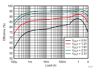
GUID-0117CAF7-DCC5-4C07-B070-18BCAB07E31D-low.gifEfficiency at VIN = 5 V