SNVSAV2B January 2018 – November 2019 TLV6700
PRODUCTION DATA.
- 1 Features
- 2 Applications
- 3 Description
- 4 Revision History
- 5 Device Comparison Table
- 6 Pin Configuration and Functions
- 7 Specifications
- 8 Detailed Description
- 9 Application and Implementation
- 10Power Supply Recommendations
- 11Layout
- 12Device and Documentation Support
- 13Mechanical, Packaging, and Orderable Information
Package Options
Mechanical Data (Package|Pins)
Thermal pad, mechanical data (Package|Pins)
Orderable Information
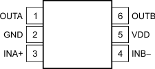
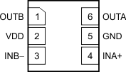
6 Pin Configuration and Functions
DDC Package
SOT-23-6
Top View

DSE Package
WSON-6
Top View

Pin Functions
| PIN | I/O | DESCRIPTION | ||
|---|---|---|---|---|
| NAME | DDC | DSE | ||
| GND | 2 | 5 | — | Ground |
| INA+ | 3 | 4 | I | This pin is connected to the voltage to be monitored with the use of an external resistor divider. When the voltage at this terminal drops below the threshold voltage (VITP – VHYS), OUTA is driven low. |
| INB– | 4 | 3 | I | This pin is connected to the voltage to be monitored with the use of an external resistor divider. When the voltage at this terminal exceeds the threshold voltage (VITP), OUTB is driven low. |
| OUTA | 1 | 6 | O | INA+ comparator open-drain output. OUTA is driven low when the voltage at this comparator is below (VITP – VHYS). The output goes high when the sense voltage returns above the respective threshold (VITP). |
| OUTB | 6 | 1 | O | INB– comparator open-drain output. OUTB is driven low when the voltage at this comparator exceeds VITP. The output goes high when the sense voltage returns below the respective threshold (VITP – VHYS). |
| VDD | 5 | 2 | I | Supply voltage input. Connect a 1.8-V to 18-V supply to VDD to power the device. Good analog design practice is to place a 0.1-µF ceramic capacitor close to this pin. |