SLVSA00E September 2009 – April 2015 TLV700
PRODUCTION DATA.
- 1 Features
- 2 Applications
- 3 Description
- 4 Revision History
- 5 Pin Configuration and Functions
- 6 Specifications
- 7 Detailed Description
- 8 Application and Implementation
- 9 Power Supply Recommendations
- 10Layout
- 11Device and Documentation Support
- 12Mechanical, Packaging, and Orderable Information
Package Options
Mechanical Data (Package|Pins)
Thermal pad, mechanical data (Package|Pins)
Orderable Information
7 Detailed Description
7.1 Overview
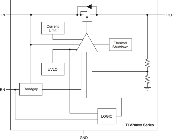
The TLV700 series of LDO linear regulators are low quiescent current devices with excellent line and load transient performance. These LDOs are designed for power-sensitive applications. A precision bandgap and error amplifier provides overall 2% accuracy. Low output noise, very high PSRR, and low dropout voltage make this series of devices ideal for most battery-operated handheld equipment. All device versions have integrated thermal shutdown, current limit, and undervoltage lockout (UVLO).
7.3 Feature Description
7.3.1 Internal Current Limit
The TLV700 internal current limit helps to protect the regulator during fault conditions. During current limit, the output sources a fixed amount of current that is largely independent of the output voltage. In such a case, the output voltage is not regulated, and is VOUT = ICL × RLOAD. The PMOS pass transistor dissipates (VIN – VOUT) × ICL until thermal shutdown is triggered and the device turns off. As the device cools down, it is turned on by the internal thermal shutdown circuit. If the fault condition continues, the device cycles between current limit and thermal shutdown. See Thermal Protection for more details.
The PMOS pass element in the TLV700 has a built-in body diode that conducts current when the voltage at OUT exceeds the voltage at IN. This current is not limited, so if extended reverse voltage operation is anticipated, external limiting to 5% of the rated output current is recommended.
7.3.2 Shutdown
The enable pin (EN) is active high. The device is enabled when voltage at EN pin goes above 0.9 V. The device is turned off when the EN pin is held at less than 0.4 V. When shutdown capability is not required, EN can be connected to the IN pin.
7.3.3 Dropout Voltage
The TLV700 uses a PMOS pass transistor to achieve low dropout. When (VIN – VOUT) is less than the dropout voltage (VDO), the PMOS pass device is in the linear region of operation and the input-to-output resistance is the RDS(on) of the PMOS pass element. VDO scales approximately with output current because the PMOS device behaves as a resistor in dropout.
As with any linear regulator, PSRR and transient response are degraded as (VIN – VOUT) approaches dropout. This effect is shown in Figure 12 in Typical Characteristics.
7.3.4 Undervoltage Lockout (UVLO)
The TLV700 uses a UVLO circuit to keep the output shut off until internal circuitry is operating properly.
7.4 Device Functional Modes
7.4.1 Normal Operation
The device regulates to the nominal output voltage under the following conditions:
- The input voltage is greater than the nominal output voltage added to the dropout voltage.
- The output current is less than the current limit.
- The input voltage is greater than the UVLO voltage.
7.4.2 Dropout Operation
If the input voltage is lower than the nominal output voltage plus the specified dropout voltage, but all other conditions are met for normal operation, the device operates in dropout mode. In this condition, the output voltage is the same the input voltage minus the dropout voltage. The transient performance of the device is significantly degraded because the pass device is in a triode state and no longer regulates the output voltage of the LDO. Line or load transients in dropout may result in large output voltage deviations.
Table 1 lists the conditions that lead to the different modes of operation.
Table 1. Device Functional Mode Comparison
| OPERATING MODE | PARAMETER | |
|---|---|---|
| VIN | IOUT | |
| Normal mode | VIN > VOUT(nom) + VDO | IOUT < ICL |
| Dropout mode | VIN < VOUT(nom) + VDO | IOUT < ICL |
| Current limit | VIN > UVLO | IOUT > ICL |
