SBVS161A november   2011  – april 2023 TLV701

PRODUCTION DATA  

  1. Features
  2. Applications
  3. Description
  4. Revision History
  5. Pin Configuration and Functions
  6. Specifications
    1. 6.1 Absolute Maximum Ratings
    2. 6.2 ESD Ratings
    3. 6.3 Recommended Operating Conditions
    4. 6.4 Thermal Information
    5. 6.5 Electrical Characteristics
    6. 6.6 Typical Characteristics
  7. Detailed Description
    1. 7.1 Overview
    2. 7.2 Functional Block Diagram
    3. 7.3 Feature Description
      1. 7.3.1 Wide Supply Range
      2. 7.3.2 Low Quiescent Current
      3. 7.3.3 Dropout Voltage (VDO)
      4. 7.3.4 Current Limit
    4. 7.4 Device Functional Modes
      1. 7.4.1 Normal Operation
      2. 7.4.2 Dropout Operation
  8. Application and Implementation
    1. 8.1 Application Information
    2. 8.2 Typical Application
      1. 8.2.1 Design Requirements
      2. 8.2.2 Detailed Design Procedure
        1. 8.2.2.1 External Capacitor Requirements
        2. 8.2.2.2 Input and Output Capacitor Requirements
        3. 8.2.2.3 Reverse Current
        4. 8.2.2.4 Power Dissipation (PD)
        5. 8.2.2.5 Estimating Junction Temperature
      3. 8.2.3 Application Curves
    3. 8.3 Best Design Practices
    4. 8.4 Power Supply Recommendations
    5. 8.5 Layout
      1. 8.5.1 Layout Guidelines
        1. 8.5.1.1 Power Dissipation
      2. 8.5.2 Layout Example
  9. Device and Documentation Support
    1. 9.1 Device Support
      1. 9.1.1 Development Support
        1. 9.1.1.1 Evaluation Module
      2. 9.1.2 Device Nomenclature
    2. 9.2 Documentation Support
      1. 9.2.1 Related Documentation
    3. 9.3 Receiving Notification of Documentation Updates
    4. 9.4 Support Resources
    5. 9.5 Trademarks
    6. 9.6 Electrostatic Discharge Caution
    7. 9.7 Glossary
  10. 10Mechanical, Packaging, and Orderable Information

Package Options

Mechanical Data (Package|Pins)
Thermal pad, mechanical data (Package|Pins)
Orderable Information

Application Curves

at operating temperature TJ = 25°C, VIN = VOUT(NOM) + 1.0 V or 2.5 V (whichever is greater), IOUT = 1 mA, CIN = 1 µF, and COUT = 1 µF (unless otherwise noted)
GUID-8F99E530-E529-4977-8F07-36C68318B2F9-low.gif
 
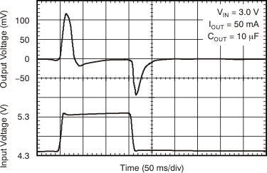
Figure 8-3 Line Transient Response for Legacy Chip
GUID-5BD511F4-D567-4520-9E14-AA696C31A9FE-low.gif
 
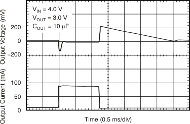
Figure 8-5 Load Transient Response for Legacy Chip
GUID-20221031-SS0I-SGTH-4LDN-CLLF5TDZ0GKX-low.svg
 
Figure 8-7 Power-Up, Power-Down for New Chip
GUID-20230108-SS0I-GGJ6-4PKG-KTFZMXZSWDR9-low.svg
 
Figure 8-4 Line Transient Response for New Chip
GUID-20230108-SS0I-PZ38-JSMQ-B1PBBGMD9VP0-low.svg
 
Figure 8-6 Load Transient Response for New Chip