SLVSE13I September   2017  – June 2024 TLV7031 , TLV7032 , TLV7034 , TLV7041 , TLV7042 , TLV7044

PRODUCTION DATA  

  1.   1
  2. Features
  3. Applications
  4. Description
  5. Pin Configuration and Functions
    1.     Pin Functions
    2.     Pin Functions: TLV7032/42
    3.     Pin Functions: TLV7034/44
  6. Specifications
    1. 5.1  Absolute Maximum Ratings
    2. 5.2  ESD Ratings
    3. 5.3  Recommended Operating Conditions
    4. 5.4  Thermal Information (Single)
    5. 5.5  Thermal Information (Dual)
    6. 5.6  Thermal Information (Quad)
    7. 5.7  Electrical Characteristics (Single)
    8. 5.8  Switching Characteristics (Single)
    9. 5.9  Electrical Characteristics (Dual)
    10. 5.10 Switching Characteristics (Dual)
    11. 5.11 Electrical Characteristics (Quad)
    12. 5.12 Switching Characteristics (Quad)
    13. 5.13 Timing Diagrams
    14. 5.14 Typical Characteristics
  7. Detailed Description
    1. 6.1 Overview
    2. 6.2 Functional Block Diagram
    3. 6.3 Feature Description
    4. 6.4 Device Functional Modes
      1. 6.4.1 Inputs
      2. 6.4.2 Internal Hysteresis
      3. 6.4.3 Output
  8. Application and Implementation
    1. 7.1 Application Information
      1. 7.1.1 Inverting Comparator With Hysteresis for TLV703x
      2. 7.1.2 Noninverting Comparator With Hysteresis for TLV703x
    2. 7.2 Typical Applications
      1. 7.2.1 Window Comparator
        1. 7.2.1.1 Design Requirements
        2. 7.2.1.2 Detailed Design Procedure
        3. 7.2.1.3 Application Curve
      2. 7.2.2 IR Receiver Analog Front End
        1. 7.2.2.1 Design Requirements
        2. 7.2.2.2 Detailed Design Procedure
        3. 7.2.2.3 Application Curve
      3. 7.2.3 Square-Wave Oscillator
        1. 7.2.3.1 Design Requirements
        2. 7.2.3.2 Detailed Design Procedure
        3. 7.2.3.3 Application Curve
      4. 7.2.4 Quadrature Rotary Encoder
        1. 7.2.4.1 Design Requirements
        2. 7.2.4.2 Detailed Design Procedure
        3. 7.2.4.3 Application Curve
    3. 7.3 Power Supply Recommendations
    4. 7.4 Layout
      1. 7.4.1 Layout Guidelines
      2. 7.4.2 Layout Example
  9. Device and Documentation Support
    1. 8.1 Device Support
      1. 8.1.1 Development Support
        1. 8.1.1.1 Evaluation Module
    2. 8.2 Documentation Support
      1. 8.2.1 Related Documentation
    3. 8.3 Receiving Notification of Documentation Updates
    4. 8.4 Support Resources
    5. 8.5 Trademarks
    6. 8.6 Electrostatic Discharge Caution
    7. 8.7 Glossary
  10. Revision History
  11. 10Mechanical, Packaging, and Orderable Information

Package Options

Mechanical Data (Package|Pins)
Thermal pad, mechanical data (Package|Pins)
Orderable Information

Inverting Comparator With Hysteresis for TLV703x

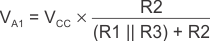
The inverting comparator with hysteresis requires a three-resistor network that is referenced to the comparator supply voltage (VCC), as shown in Figure 7-1. When VIN at the inverting input is less than VA, the output voltage is high (for simplicity, assume VO switches as high as VCC). The three network resistors can be represented as R1 || R3 in series with R2. Equation 1 defines the high-to-low trip voltage (VA1).

Equation 1. TLV7031 TLV7032 TLV7041 TLV7042 TLV7034 TLV7044

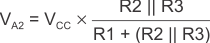
When VIN is greater than VA, the output voltage is low, very close to ground. In this case, the three network resistors can be presented as R2 || R3 in series with R1. Use Equation 2 to define the low to high trip voltage (VA2).

Equation 2. TLV7031 TLV7032 TLV7041 TLV7042 TLV7034 TLV7044

Equation 3 defines the total hysteresis provided by the network.

Equation 3. TLV7031 TLV7032 TLV7041 TLV7042 TLV7034 TLV7044
TLV7031 TLV7032 TLV7041 TLV7042 TLV7034 TLV7044 TLV703x in an Inverting Configuration With Hysteresis
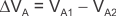
Figure 7-1 TLV703x in an Inverting Configuration With Hysteresis