SLVSE13I September 2017 – June 2024 TLV7031 , TLV7032 , TLV7034 , TLV7041 , TLV7042 , TLV7044
PRODUCTION DATA
- 1
- 1 Features
- 2 Applications
- 3 Description
- 4 Pin Configuration and Functions
-
5 Specifications
- 5.1 Absolute Maximum Ratings
- 5.2 ESD Ratings
- 5.3 Recommended Operating Conditions
- 5.4 Thermal Information (Single)
- 5.5 Thermal Information (Dual)
- 5.6 Thermal Information (Quad)
- 5.7 Electrical Characteristics (Single)
- 5.8 Switching Characteristics (Single)
- 5.9 Electrical Characteristics (Dual)
- 5.10 Switching Characteristics (Dual)
- 5.11 Electrical Characteristics (Quad)
- 5.12 Switching Characteristics (Quad)
- 5.13 Timing Diagrams
- 5.14 Typical Characteristics
- 6 Detailed Description
- 7 Application and Implementation
- 8 Device and Documentation Support
- 9 Revision History
- 10Mechanical, Packaging, and Orderable Information
Package Options
Mechanical Data (Package|Pins)
Thermal pad, mechanical data (Package|Pins)
Orderable Information
Pin Functions
Table 4-1 Pin Functions: TLV70x1,
TLV70x1L, and TLV70x1S
| NAME | TLV7031, TLV7041 | TLV7031L, TLV7041L | TLV7031S, TLV7041S | I/O | DESCRIPTION | |||
|---|---|---|---|---|---|---|---|---|
| PINS | PINS | PINS | ||||||
| SOT-23 | SC-70 | X2SON | SOT-23 | SOT-23 | SC-70 | |||
| OUT | 1 | 1 | 1 | 1 | 4 | 4 | O | Output |
| V- | 2 | 2 | 3 | 5 | 2 | 2 | - | Negative Supply Voltage |
| IN+ | 3 | 3 | 5 | 3 | 1 | 1 | I | Non-Inverting (+) Input |
| IN- | 4 | 4 | 4 | 4 | 3 | 3 | I | Inverting (-) Input |
| V+ | 5 | 5 | 2 | 2 | 5 | 5 | - | Positive Supply Voltage |
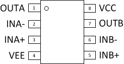
 Figure 4-5 TLV7032/42 DGK,
DDF Packages
Figure 4-5 TLV7032/42 DGK,
DDF Packages8-Pin VSSOP, SOT-23
Top View

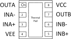
A. Connect thermal pad to V–.
Figure 4-6 TLV7032/42 DSG
Package8-Pin WSON With Exposed Thermal Pad
Top View