SLVSE13J September 2017 – November 2024 TLV7031 , TLV7032 , TLV7034 , TLV7041 , TLV7042 , TLV7044
PRODUCTION DATA
- 1
- 1 Features
- 2 Applications
- 3 Description
- 4 Pin Configuration and Functions
-
5 Specifications
- 5.1 Absolute Maximum Ratings
- 5.2 ESD Ratings
- 5.3 Recommended Operating Conditions
- 5.4 Thermal Information (Single)
- 5.5 Thermal Information (Dual)
- 5.6 Thermal Information (Quad)
- 5.7 Electrical Characteristics (Single)
- 5.8 Switching Characteristics (Single)
- 5.9 Electrical Characteristics (Dual)
- 5.10 Switching Characteristics (Dual)
- 5.11 Electrical Characteristics (Quad)
- 5.12 Switching Characteristics (Quad)
- 5.13 Timing Diagrams
- 5.14 Typical Characteristics
- 6 Detailed Description
- 7 Application and Implementation
- 8 Device and Documentation Support
- 9 Revision History
- 10Mechanical, Packaging, and Orderable Information
Package Options
Mechanical Data (Package|Pins)
Thermal pad, mechanical data (Package|Pins)
- DPW|5
Orderable Information
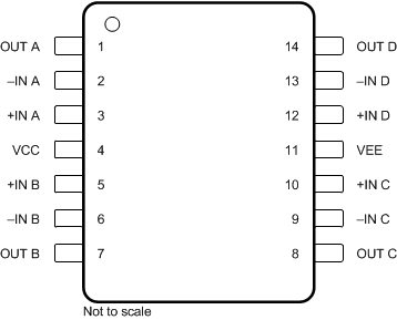
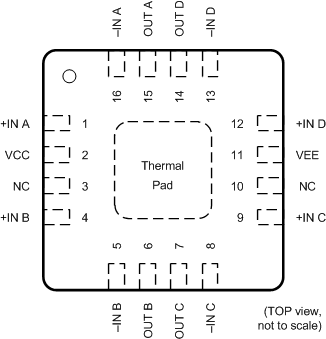
4.3 Pin Functions: TLV7034/44 Quad
 Figure 4-7 Figure 4-7 TLV7034/44 PW Packages 14-Pin TSSOP Top View |  A. Connect thermal pad to V–. Figure 4-8 TLV7034/44 RTE Package 16-Pin WQFN With Exposed Thermal Pad Top View |
Table 4-3 Pin Functions
| PIN | I/O | DESCRIPTION | ||
|---|---|---|---|---|
| NAME | TSSOP | WQFN | ||
| –IN1 A | 2 | 16 | I | Inverting input, channel A |
| +IN A | 3 | 1 | I | Noninverting input, channel A |
| –IN B | 6 | 5 | I | Inverting input, channel B |
| +IN B | 5 | 4 | I | Noninverting input, channel B |
| –IN C | 9 | 8 | I | Inverting input, channel C |
| +IN C | 10 | 9 | I | Noninverting input, channel C |
| –IN D | 13 | 13 | I | Inverting input, channel D |
| +IN D | 12 | 12 | I | Noninverting input, channel D |
| NC | — | 3, 10 | — | No internal connection |
| OUT A | 1 | 15 | O | Output, channel A |
| OUT B | 7 | 6 | O | Output, channel B |
| OUT C | 8 | 7 | O | Output, channel C |
| OUT D | 14 | 14 | O | Output, channel D |
| VEE | 11 | 11 | — | Negative (lowest) supply or ground (for single-supply operation) |
| VCC | 4 | 2 | — | Positive (highest) supply |