SLVSE13J September 2017 – November 2024 TLV7031 , TLV7032 , TLV7034 , TLV7041 , TLV7042 , TLV7044
PRODUCTION DATA
- 1
- 1 Features
- 2 Applications
- 3 Description
- 4 Pin Configuration and Functions
-
5 Specifications
- 5.1 Absolute Maximum Ratings
- 5.2 ESD Ratings
- 5.3 Recommended Operating Conditions
- 5.4 Thermal Information (Single)
- 5.5 Thermal Information (Dual)
- 5.6 Thermal Information (Quad)
- 5.7 Electrical Characteristics (Single)
- 5.8 Switching Characteristics (Single)
- 5.9 Electrical Characteristics (Dual)
- 5.10 Switching Characteristics (Dual)
- 5.11 Electrical Characteristics (Quad)
- 5.12 Switching Characteristics (Quad)
- 5.13 Timing Diagrams
- 5.14 Typical Characteristics
- 6 Detailed Description
- 7 Application and Implementation
- 8 Device and Documentation Support
- 9 Revision History
- 10Mechanical, Packaging, and Orderable Information
Package Options
Mechanical Data (Package|Pins)
Thermal pad, mechanical data (Package|Pins)
- DPW|5
Orderable Information
3 Description
The TLV7031/41 (single-channel), TLV7032/42 (dual-channel), and TLV7034/44 (quad-channel) are low-voltage, nanoPower comparators. These devices are available in an ultra-small, leadless packages as well as standard 5-pin SC70, SOT-23, VSSOP, and TSSOP packages, making them applicable for space-critical designs like smartphones, smart meters, and other portable or battery-powered applications.
The TLV703x and TLV704x offer an excellent combination of speed and power, with a propagation delay of 3μs and a quiescent supply current of 315nA. The benefit of fast response time at nanoPower enables power-conscious systems to monitor and respond quickly to fault conditions. With an operating voltage range of 1.6V to 6.5V, these comparators are compatible with 3V and 5V systems.
The TLV703x and TLV704x is designed for no output phase inversion with overdriven inputs and internal hysteresis, so engineers can use this family of comparators for precision voltage monitoring in harsh, noisy environments where slow-moving input signals must be converted into clean digital outputs.
The TLV703x has a push-pull output stage capable of sinking and sourcing milliamps of current when controlling an LED or driving a capacitive load. The TLV704x has an open-drain output stage that can be pulled beyond VCC, making the device an excellent chice for level translators and bipolar to single-ended converters. The "S" and "L" options are alternate single pinouts with 1.2 minimum supply voltage.
| PART NUMBERS | PACKAGE (PINS) (1) | BODY SIZE (NOM) (2) |
|---|---|---|
| TLV7031, TLV7041 | SOT-23 (5) | 2.90mm × 1.60mm |
| SC70 (5) | 2.00mm × 1.25mm | |
| X2SON (5) | 0.80mm × 0.80mm | |
| TLV7031L, TLV7041L | SOT-23 (5) | 2.90mm × 1.60mm |
| TLV7031S, TLV7041S | SC70 (5) | 2.00mm × 1.25mm |
| SOT-23 (5) | 2.90mm × 1.60mm | |
| TLV7032, TLV7042 | VSSOP (8) | 3.00mm x 3.00mm |
| SOT-23 (8) | 2.90mm x 1.60mm | |
| WSON (8) | 2.00mm x 2.00mm | |
| TLV7034, TLV7044 | WQFN (16) | 3.00mm x 3.00mm |
| TSSOP (14) | 4.40mm x 5.00mm |
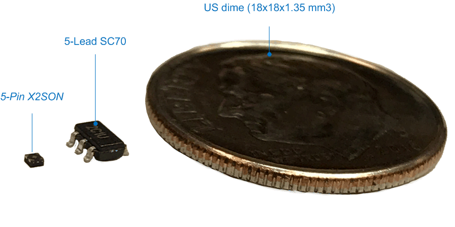
 X2SON Package vs SC70 and US Dime
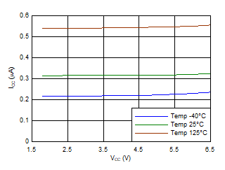
 ICC vs. Supply Voltage for Dual