SLVSE13J September   2017  – November 2024 TLV7031 , TLV7032 , TLV7034 , TLV7041 , TLV7042 , TLV7044

PRODUCTION DATA  

  1.   1
  2. Features
  3. Applications
  4. Description
  5. Pin Configuration and Functions
    1. 4.1 Pin Functions: TLV7031/41 Singles including "S" and "L" options
    2. 4.2 Pin Functions: TLV7032/42 Dual
    3. 4.3 Pin Functions: TLV7034/44 Quad
  6. Specifications
    1. 5.1  Absolute Maximum Ratings
    2. 5.2  ESD Ratings
    3. 5.3  Recommended Operating Conditions
    4. 5.4  Thermal Information (Single)
    5. 5.5  Thermal Information (Dual)
    6. 5.6  Thermal Information (Quad)
    7. 5.7  Electrical Characteristics (Single)
    8. 5.8  Switching Characteristics (Single)
    9. 5.9  Electrical Characteristics (Dual)
    10. 5.10 Switching Characteristics (Dual)
    11. 5.11 Electrical Characteristics (Quad)
    12. 5.12 Switching Characteristics (Quad)
    13. 5.13 Timing Diagrams
    14. 5.14 Typical Characteristics
  7. Detailed Description
    1. 6.1 Overview
    2. 6.2 Functional Block Diagram
    3. 6.3 Feature Description
    4. 6.4 Device Functional Modes
      1. 6.4.1 Inputs
      2. 6.4.2 Internal Hysteresis
      3. 6.4.3 Output
  8. Application and Implementation
    1. 7.1 Application Information
      1. 7.1.1 Inverting Comparator With Hysteresis for TLV703x
      2. 7.1.2 Non-Inverting Comparator With Hysteresis for TLV703x
    2. 7.2 Typical Applications
      1. 7.2.1 Window Comparator
        1. 7.2.1.1 Design Requirements
        2. 7.2.1.2 Detailed Design Procedure
        3. 7.2.1.3 Application Curve
      2. 7.2.2 IR Receiver Analog Front End
        1. 7.2.2.1 Design Requirements
        2. 7.2.2.2 Detailed Design Procedure
        3. 7.2.2.3 Application Curve
      3. 7.2.3 Square-Wave Oscillator
        1. 7.2.3.1 Design Requirements
        2. 7.2.3.2 Detailed Design Procedure
        3. 7.2.3.3 Application Curve
      4. 7.2.4 Quadrature Rotary Encoder
        1. 7.2.4.1 Design Requirements
        2. 7.2.4.2 Detailed Design Procedure
        3. 7.2.4.3 Application Curve
    3. 7.3 Power Supply Recommendations
    4. 7.4 Layout
      1. 7.4.1 Layout Guidelines
      2. 7.4.2 Layout Example
  9. Device and Documentation Support
    1. 8.1 Device Support
      1. 8.1.1 Development Support
        1. 8.1.1.1 Evaluation Module
    2. 8.2 Documentation Support
      1. 8.2.1 Related Documentation
    3. 8.3 Receiving Notification of Documentation Updates
    4. 8.4 Support Resources
    5. 8.5 Trademarks
    6. 8.6 Electrostatic Discharge Caution
    7. 8.7 Glossary
  10. Revision History
  11. 10Mechanical, Packaging, and Orderable Information

Package Options

Mechanical Data (Package|Pins)
Thermal pad, mechanical data (Package|Pins)
Orderable Information

Non-Inverting Comparator With Hysteresis for TLV703x

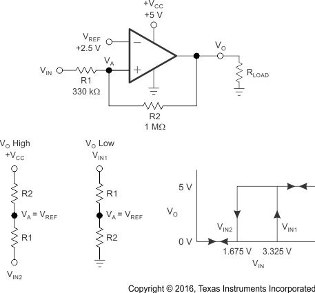
A noninverting comparator with hysteresis requires a two-resistor network, as shown in Figure 7-2, and a voltage reference (VREF) at the inverting input. When VIN is low, the output is also low. For the output to switch from low to high, VIN must rise to VIN1. Use Equation 4 to calculate VIN1.

Equation 4. TLV7031 TLV7032 TLV7041 TLV7042 TLV7034 TLV7044

When VIN is high, the output is also high. For the comparator to switch back to a low state, VIN must drop to VIN2 such that VA is equal to VREF. Use Equation 5 to calculate VIN2.

Equation 5. TLV7031 TLV7032 TLV7041 TLV7042 TLV7034 TLV7044

The hysteresis of this circuit is the difference between VIN1 and VIN2, as shown in Equation 6.

Equation 6. TLV7031 TLV7032 TLV7041 TLV7042 TLV7034 TLV7044
TLV7031 TLV7032 TLV7041 TLV7042 TLV7034 TLV7044 TLV703x in a Noninverting Configuration With HysteresisFigure 7-2 TLV703x in a Noninverting Configuration With Hysteresis