SBVS266 May 2015 TLV713P-Q1
PRODUCTION DATA.
- 1 Features
- 2 Applications
- 3 Description
- 4 Revision History
- 5 Pin Configurations and Functions
- 6 Specifications
- 7 Detailed Description
- 8 Application and Implementation
- 9 Power-Supply Recommendations
- 10Layout
- 11Device and Documentation Support
- 12Mechanical, Packaging, and Orderable Information
Package Options
Mechanical Data (Package|Pins)
- DBV|5
Thermal pad, mechanical data (Package|Pins)
Orderable Information
8 Application and Implementation
NOTE
Information in the following applications sections is not part of the TI component specification, and TI does not warrant its accuracy or completeness. TI’s customers are responsible for determining suitability of components for their purposes. Customers should validate and test their design implementation to confirm system functionality.
8.1 Application Information
8.1.1 Input and Output Capacitor Considerations
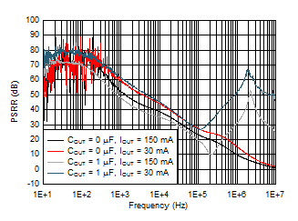
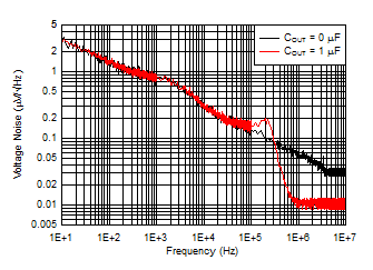
The TLV713P-Q1 uses an advanced internal control loop to obtain stable operation both with and without the use of input or output capacitors. The TLV713P-Q1 dynamic performance is improved with the use of an output capacitor. An output capacitance of 0.1 μF or larger generally provides good dynamic response. X5R- and X7R-type ceramic capacitors are recommended because these capacitors have minimal variation in value and equivalent series resistance (ESR) over temperature.
Although an input capacitor is not required for stability, good analog design practice is to connect a 0.1-µF to
1-µF capacitor from IN to GND. This capacitor counteracts reactive input sources and improves transient response, input ripple, and PSRR. An input capacitor is recommended if the source impedance is more than
0.5 Ω. A higher-value capacitor may be necessary if large, fast, rise-time load transients are anticipated or if the device is located several inches from the input power source.
8.1.2 Dropout Voltage
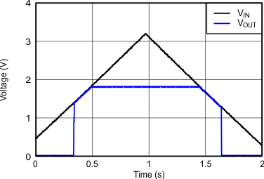
The TLV713P-Q1 uses a PMOS pass transistor to achieve low dropout. When (VIN – VOUT) is less than the dropout voltage (VDO), the PMOS pass device is in the linear region of operation and the input-to-output resistance is the RDS(on) of the PMOS pass element. VDO scales approximately with output current because the PMOS device behaves like a resistor in dropout. As with any linear regulator, PSRR and transient response are degraded when (VIN – VOUT) approaches dropout.
8.1.3 Transient Response
As with any regulator, increasing the size of the output capacitor reduces over- and undershoot magnitude but increases the duration of the transient response.
8.2 Typical Application
Several versions of the TPS713P-Q1 are ideal for powering the MSP430 microcontroller.
Figure 24 shows a diagram of the TLV713P-Q1 powering an MSP430 microcontroller. Table 2 shows potential applications of some voltage versions.
 Figure 24. TLV713P-Q1 Powering a Microcontroller
Table 2. Typical MSP430 Applications
| DEVICE | VOUT (Typ) | APPLICATION |
|---|---|---|
| TLV71318P-Q1 | 1.8 V | Allows for lowest power consumption with many MSP430s |
| TLV71325P-Q1 | 2.5 V | 2.2-V supply required by many MSP430s for flash programming and erasing |
8.2.1 Design Requirements
Table 3 lists the design requirements.
Table 3. Design Parameters
| PARAMETER | DESIGN REQUIREMENT |
|---|---|
| Input voltage | 4.2 V to 3 V (Lithium Ion battery) |
| Output voltage | 1.8 V, ±1% |
| DC output current | 10 mA |
| Peak output current | 75 mA |
| Maximum ambient temperature | 65°C |
8.2.2 Detailed Design Procedure
An input capacitor is not required for this design because of the low impedance connection directly to the battery.
No output capacitor allows for the minimal possible inrush current during start-up, ensuring the 180-mA maximum input current limit is not exceeded.
8.2.3 Application Curves


| IOUT = 150 mA |

8.3 Do's and Don'ts
For best transient performance, place at least one 0.1-µF ceramic capacitor as close as possible to the OUT pin of the regulator and at least one 1-uF capacitor as close as possible to the IN pin of the regulator.
Do not place the output capacitor more than 10 mm away from the regulator.
Do not exceed the absolute maximum ratings.
Do not continuously operate the device in current limit or near thermal shutdown.