SBVS217B June 2013 – November 2015 TLV716P
PRODUCTION DATA.
- 1 Features
- 2 Applications
- 3 Description
- 4 Revision History
- 5 Pin Configuration and Functions
- 6 Specifications
- 7 Detailed Description
- 8 Application and Implementation
- 9 Power Supply Recommendations
- 10Layout
- 11Device and Documentation Support
- 12Mechanical, Packaging, and Orderable Information
Package Options
Mechanical Data (Package|Pins)
- DPQ|6
Thermal pad, mechanical data (Package|Pins)
- DPQ|6
Orderable Information
7 Detailed Description
7.1 Overview
The TLV716 and TLV716P devices belong to a new family of next-generation of dual-value, low-dropout (LDO) regulators. These devices consume low quiescent current and deliver excellent line and load transient performance. These characteristics, combined with low noise, very good PSRR with little (VIN – VOUT) headroom, make this family of devices ideal for RF portable applications.
This family of regulators offers current limit and thermal protection. Device operating junction temperature is –40°C to 125°C.
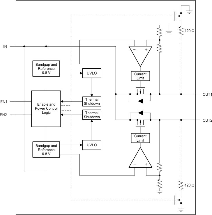
7.2 Functional Block Diagram

NOINDENT:
NOTE: Dashed lines are for the TLV716P only.7.3 Feature Description
7.3.1 Internal Current Limit
The TLV716 and TLV716P have an internal foldback current limit that helps protect the regulator during fault conditions. The current supplied by the device gradually reduces while the output voltage decreases. When the output is connected to ground, the LDO supplies a typical current of 40 mA. When in current limit, the output voltage is not regulated and VOUT = IOUT × RLOAD; see Figure 10 and Figure 11. The PMOS pass transistor dissipates [(VIN – VOUT) × ILIMIT] until thermal shutdown is triggered and the device turns off. When the device cools down, the internal thermal shutdown circuit turns on the device. If the fault condition continues, the device cycles between current limit and thermal shutdown. See the Thermal Considerations section for more details.
The TLV716 PMOS pass element has a built-in body diode that conducts current when the voltage at OUT exceeds the voltage at IN. This current is not limited, so if extended reverse voltage operation is anticipated, external limiting to 5% of the rated output current is recommended. A small schottky diode connected with the anode to OUT and the cathode to IN can accomplish this limiting.
7.3.2 Shutdown
The enable pin (EN) is active high. The device is enabled when the EN pin goes above 0.9 V. This relatively low value of voltage required to turn the LDO regulator on can be used to enable the device with the general-purpose input/output (GPIO) of recent processors whose GPIO voltage is lower than traditional microcontrollers.
The device is turned off when the EN pin is held at less than 0.4 V. When shutdown capability is not required, the EN pin can connected to the IN pin. The TLV716P will pull down the output with a 120-Ω resistor when the EN pin falls below 0.4 V.
7.3.3 Undervoltage Lockout (UVLO)
The TLV716 and TLV716P use an undervoltage lockout circuit (1.3 V, typical) to keep the output shut off until the internal circuitry is operating properly.
7.4 Device Functional Modes
7.4.1 Capacitor-Free Operation
The TLV716 and TLV716P are stable without the use of input or output capacitors. This functionality results in a reduction of component count, cost, and solution size. In addition, without the need of external capacitors, the ultra-small, 1.2-mm × 1.2-mm DPQ package optimizes the solution size for board space-constrained applications. To optimize device AC performance, an input and output capacitor is recommended, as described in the Input and Output Capacitor Requirements section.