SBVS320D November 2017 – September 2024 TLV755P
PRODUCTION DATA
- 1
- 1 Features
- 2 Applications
- 3 Description
- 4 Pin Configuration and Functions
- 5 Specifications
- 6 Detailed Description
- 7 Application and Implementation
- 8 Device and Documentation Support
- 9 Revision History
- 10Mechanical, Packaging, and Orderable Information
Package Options
Refer to the PDF data sheet for device specific package drawings
Mechanical Data (Package|Pins)
- DYD|5
- DBV|5
- DQN|4
- DRV|6
Thermal pad, mechanical data (Package|Pins)
Orderable Information
7.1.4 Reverse Current
As with most LDOs, excessive reverse current potentially damages this device.
Reverse current flows through the body diode on the pass transistor instead of the normal conducting channel. At high magnitudes, this current flow degrades the long-term reliability of the device, as a result of one of the following conditions:
- Degradation caused by electromigration
- Excessive heat dissipation
- Potential for a latch-up condition
Conditions where reverse current occur are outlined in this section, all of which exceed the absolute maximum rating of VOUT > VIN + 0.3V:
- If the device has a large COUT and the input supply collapses with little or no load current
- The output is biased when the input supply is not established
- The output is biased above the input supply
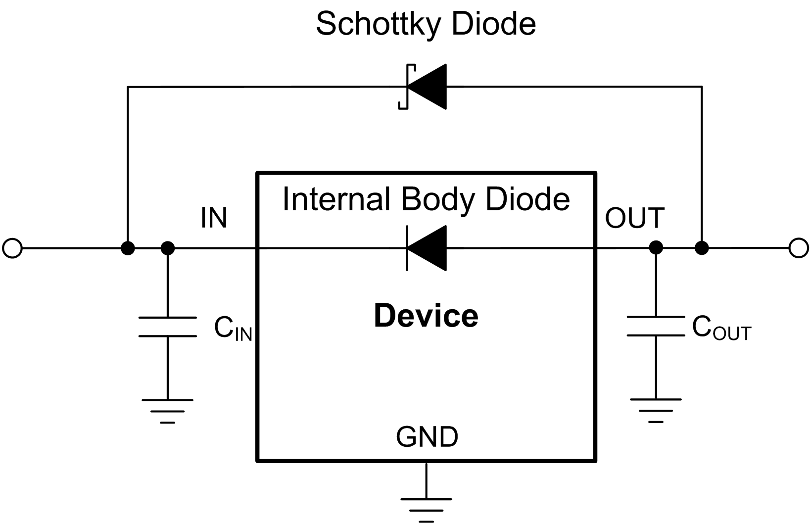
If reverse current flow is expected in the application, use external protection to protect the device. Figure 7-3 shows one approach of protecting the device.
 Figure 7-3 Example Circuit for Reverse Current Protection Using a Schottky Diode