SBVS351D April   2018  – October 2023 TLV758P

PRODUCTION DATA  

  1.   1
  2. Features
  3. Applications
  4. Description
  5. Pin Configuration and Functions
  6. Specifications
    1. 5.1 Absolute Maximum Ratings
    2. 5.2 ESD Ratings
    3. 5.3 Recommended Operating Conditions
    4. 5.4 Thermal Information
    5. 5.5 Electrical Characteristics
    6. 5.6 Typical Characteristics
  7. Detailed Description
    1. 6.1 Overview
    2. 6.2 Functional Block Diagram
    3. 6.3 Feature Description
      1. 6.3.1 Undervoltage Lockout (UVLO)
      2. 6.3.2 Shutdown
      3. 6.3.3 Foldback Current Limit
      4. 6.3.4 Thermal Shutdown
    4. 6.4 Device Functional Modes
      1. 6.4.1 Device Functional Mode Comparison
      2. 6.4.2 Normal Operation
      3. 6.4.3 Dropout Operation
      4. 6.4.4 Disabled
  8. Application and Implementation
    1. 7.1 Application Information
      1. 7.1.1 Adjustable Device Feedback Resistors
      2. 7.1.2 Input and Output Capacitor Selection
      3. 7.1.3 Dropout Voltage
      4. 7.1.4 Exiting Dropout
      5. 7.1.5 Reverse Current
      6. 7.1.6 Power Dissipation (PD)
      7. 7.1.7 Feed-Forward Capacitor (CFF)
      8. 7.1.8 Start-Up Sequencing
    2. 7.2 Typical Application
      1. 7.2.1 Design Requirements
      2. 7.2.2 Detailed Design Procedure
        1. 7.2.2.1 Input Current
        2. 7.2.2.2 Thermal Dissipation
      3. 7.2.3 Application Curve
    3. 7.3 Power Supply Recommendations
    4. 7.4 Layout
      1. 7.4.1 Layout Guidelines
      2. 7.4.2 Layout Examples
  9. Device and Documentation Support
    1. 8.1 Documentation Support
      1. 8.1.1 Device Nomenclature
      2. 8.1.2 Related Documentation
    2. 8.2 Receiving Notification of Documentation Updates
    3. 8.3 Support Resources
    4. 8.4 Trademarks
    5. 8.5 Electrostatic Discharge Caution
    6. 8.6 Glossary
  10. Revision History
  11. 10Mechanical, Packaging, and Orderable Information

Package Options

Mechanical Data (Package|Pins)
Thermal pad, mechanical data (Package|Pins)
Orderable Information

Typical Characteristics

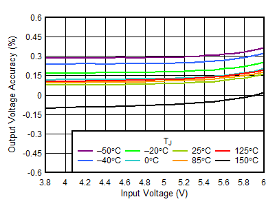
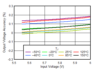
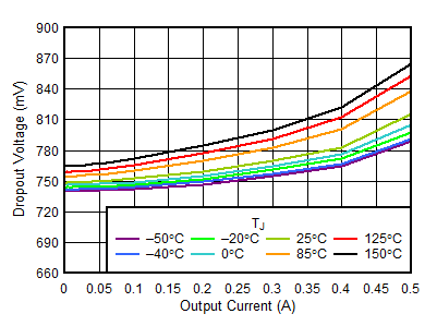
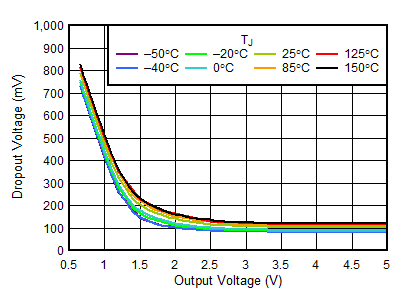
at operating temperature range TJ = 25°C, VIN = VOUT(NOM) + 0.5 V or 1.5 V (whichever is greater), IOUT = 1 mA, VEN = VIN, and CIN = COUT = 1 µF (unless otherwise noted)
GUID-68F14633-AE73-417E-B158-E24EC44B1E53-low.gif
VOUT = 3.3 V, IOUT = 1 mA
Figure 5-1 3.3-V Line Regulation vs VIN
GUID-298FA8F9-189C-4010-82FE-51BD4E1290E3-low.gif
VOUT = 5.5 V, IOUT = 1 mA
Figure 5-3 5.5-V Line Regulation vs VIN
GUID-B4D9425C-9E66-480C-B16B-3BB994BC9501-low.gif
 
Figure 5-5 0.55-V Dropout Voltage vs IOUT
GUID-31AE8E51-A4F7-4D2D-8984-F9576A977C3C-low.gif
IOUT = 500 mA
Figure 5-7 VDO vs VOUT
GUID-5DBC97AC-B842-4472-A571-B2DF7F34E01E-low.gif
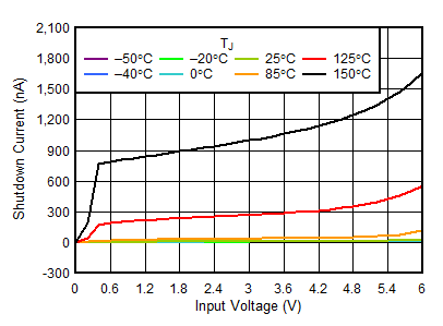
VEN = 0 V
Figure 5-9 ISHDN vs VIN
GUID-51A0B003-73E1-471F-9182-21153D7FE8D4-low.gif
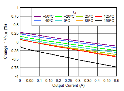
VIN = 3.8 V, VOUT = 3.3 V
Figure 5-11 3.3-V Load Regulation vs IOUT
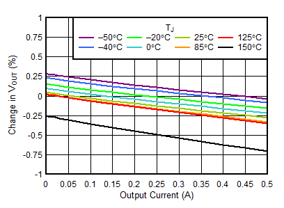
GUID-3950ED05-F9BB-406D-B83F-948613E0E0A7-low.gif
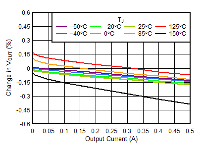
VIN = 6 V, VOUT = 5.5 V
Figure 5-13 5.5-V Load Regulation vs IOUT
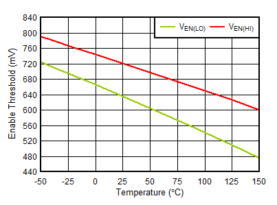
GUID-536B27E4-17DE-4BFA-9D1F-E47291C9BF30-low.gif
 
Figure 5-15 VEN(HI) and VEN(LO) vs Temperature
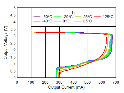
GUID-BAEA2BB2-4ECF-49D8-81B2-F2EE24CA642F-low.gif
 
Figure 5-17 3.3-V Foldback Current Limit vs IOUT
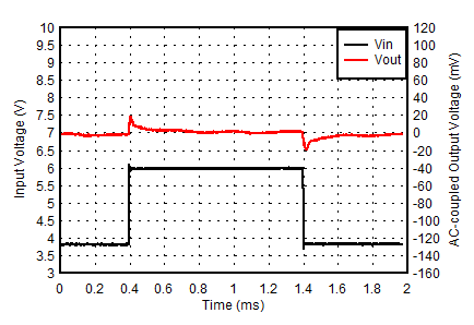
GUID-85944DC4-A826-486E-8211-C65B034F5895-low.gif
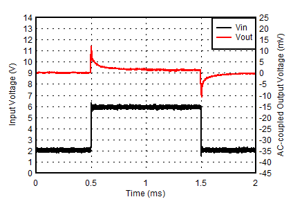
VOUT = 3.3 V, IOUT = 1 mA, VIN slew rate = 1 V/µs
Figure 5-19 3.3-V Line Transient
GUID-BAA29233-0160-4226-A2C7-9CE1ABA39A16-low.gif
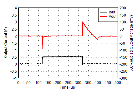
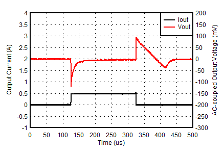
VIN = 2 V, VOUT = 0.55 V, IOUT slew rate = 1 A/µs
Figure 5-21 0.55-V, 1-mA to 500-mA Load Transient
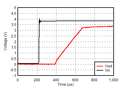
GUID-FB0C5B16-B0ED-4534-8EE0-83E6A0D175D2-low.gif
VIN = 3.8 V, VOUT = 3.3 V, IOUT = 1 mA
Figure 5-23 VIN Power-Up
GUID-FA2502D9-43BA-4260-8E7D-0967A6166DCB-low.gif
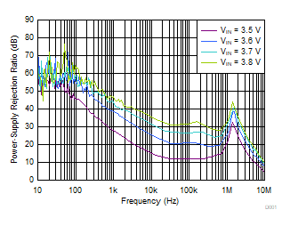
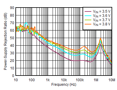
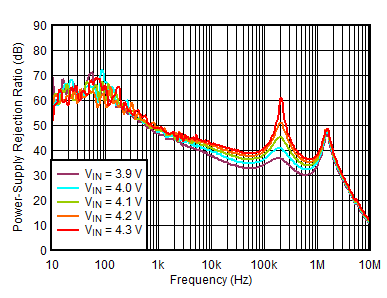
VOUT = 3.3 V, IOUT = 500 mA, COUT = 2.2 µF
Figure 5-25 PSRR vs Frequency and VIN
GUID-17FC1E1A-E22F-41EC-833E-BAC968E059EF-low.gif
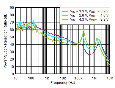
VOUT = 3.3 V, IOUT = 250 mA, COUT = 2.2 µF
Figure 5-27 PSRR vs Frequency and VIN
GUID-12A7C7E1-AFB3-47E3-AC7B-B457773AA29E-low.gif
IOUT = 500 mA, COUT = 2.2 µF
Figure 5-29 PSRR vs Frequency
GUID-FCBD8027-3C41-4F2B-BACB-66FBD041F934-low.gif
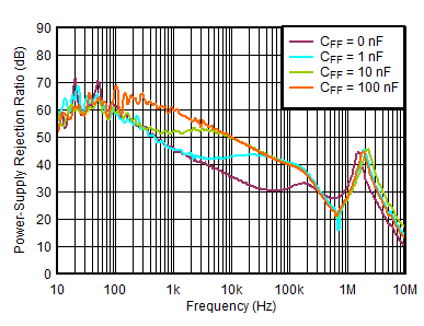
VIN = 3.8 V, VOUT = 3.3 V, IOUT = 500 mA
Figure 5-31 PSRR vs Frequency and CFF
GUID-45B7B2D3-8957-471B-8719-3E7483D0178C-low.gif
VIN = 3.8 V, VOUT = 3.3 V, COUT = 2.2 µF, VRMS BW = 10 Hz to 100 kHz
Figure 5-33 Output Spectral Noise Density
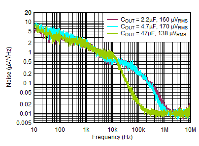
GUID-01FEF41B-8114-4279-B0F0-B1CA65ED0F20-low.gif
VIN = 3.8 V, VOUT = 3.3 V, IOUT = 100 mA, CFF = 0 µF, VRMS BW = 10 Hz to 100 kHz
Figure 5-35 Output Spectral Noise Density vs Frequency and COUT
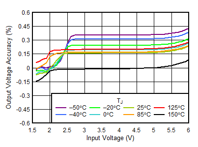
GUID-D85087F7-55A7-4A5D-840C-9AF0E99FE4D8-low.gif
VOUT = 0.55 V, IOUT = 1 mA
Figure 5-2 0.55-V Line Regulation vs VIN
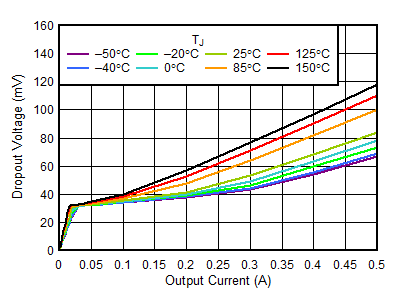
GUID-15AD6D28-4FD7-4B68-9B5C-3C6DBD1D6B2E-low.gif
 
Figure 5-4 3.3-V Dropout Voltage vs IOUT
GUID-7B01E915-AE0B-4EB0-902F-C4BABF7605CC-low.gif
 
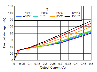
Figure 5-6 5.5-V Dropout Voltage vs IOUT
GUID-E56BBCC2-1682-4E39-98E2-2A8E27967B6A-low.gif
 
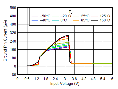
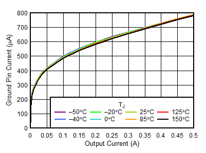
Figure 5-8 IGND vs IOUT
GUID-B80EDBF4-FCB5-4A1E-BD86-90EBE7956B5D-low.gif
VOUT = 3.3 V, IOUT = 0 mA
Figure 5-10 IQ vs VIN
GUID-69FDA44D-E31A-4B2B-A765-9A48C638EFF7-low.gif
VIN = 2 V, VOUT = 0.55 V
Figure 5-12 0.55-V Load Regulation vs IOUT
GUID-58A3BAC2-2772-4496-A2D3-DE388BB58644-low.gif
 
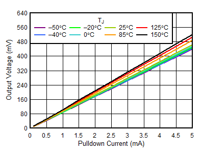
Figure 5-14 VOUT vs IOUT Pulldown Resistor
GUID-BF9E1012-6CDF-4BCC-8227-EE5E398E3A0B-low.gif
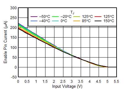
VEN = 5.5 V
Figure 5-16 IEN vs VIN
GUID-B1CDC2C2-966A-4363-A916-1ECA19638753-low.gif
VOUT = 0.55 V, IOUT = 1 mA, VIN slew rate = 1 V/µs
Figure 5-18 0.55-V Line Transient
GUID-5F67490C-A18A-42E5-9FBC-BB2152A48B55-low.gif
VIN = 3.8 V, VOUT = 3.3 V, IOUT slew rate = 1 A/µs
Figure 5-20 3.3-V, 1-mA to 500-mA Load Transient
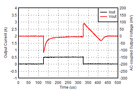
GUID-8A0216C1-AE09-4A44-91F3-FB73883B3336-low.gif
VIN = 5.5 V, VOUT = 5 V, IOUT slew rate = 1 A/µs
Figure 5-22 5-V, 1-mA to 500-mA Load Transient
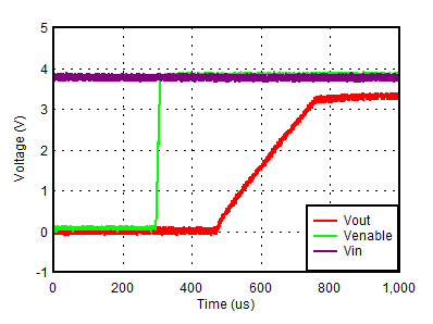
GUID-D09F5568-6F50-4A6F-A697-E537C8BACD46-low.gif
VIN = 3.8 V, VOUT = 3.3 V, IOUT = 1 mA
Figure 5-24 Start-Up With EN
GUID-0F8FD331-6CD2-4474-8729-7564ACED6A6D-low.gif
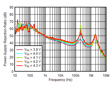
VOUT = 3.3 V, IOUT = 500 mA, COUT = 2.2 µF
Figure 5-26 PSRR vs Frequency and VIN
GUID-4125A3B3-28D7-4986-AC15-9EE7C79C0809-low.gif
VOUT = 3.3 V, IOUT = 250 mA, COUT = 2.2 µF
Figure 5-28 PSRR vs Frequency and VIN
GUID-BE5C6805-CD8E-4DC4-8DD6-FEC4D7FE3757-low.gif
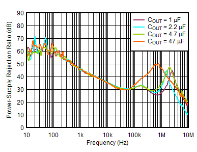
VIN = 3.8 V, VOUT = 3.3 V, IOUT = 500 mA
Figure 5-30 PSRR vs Frequency and COUT
GUID-CB87CAEE-1375-4011-A7EA-2A40F5284E97-low.gif
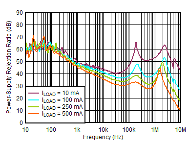
VIN = 3.8 V, VOUT = 3.3 V, COUT = 2.2 µF
Figure 5-32 PSRR vs Frequency and ILOAD
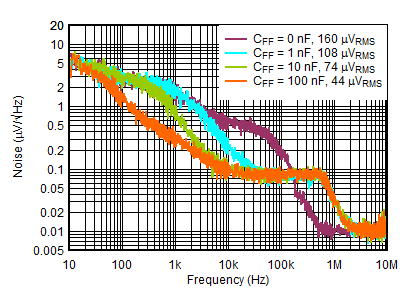
GUID-5948C06C-026A-4DDA-87F9-351B41D48804-low.gif
VIN = 3.8 V, VOUT = 3.3 V, IOUT = 500 mA, COUT = 2.2 µF, VRMS BW = 10 Hz to 100 kHz
Figure 5-34 Output Spectral Noise Density vs Frequency and CFF
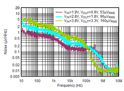
GUID-F492157F-3B4D-430F-A906-D8A6B692D9AE-low.gif
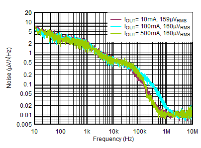
IOUT = 500 mA, COUT = 2.2 µF, VRMS BW = 10 Hz to 100 kHz
 
Figure 5-36 Output Spectral Noise Density vs Frequency