SBVS352A April 2018 – December 2018 TLV759P
PRODUCTION DATA.
- 1 Features
- 2 Applications
- 3 Description
- 4 Revision History
- 5 Pin Configuration and Functions
- 6 Specifications
- 7 Detailed Description
- 8 Application and Implementation
- 9 Power Supply Recommendations
- 10Layout
- 11Device and Documentation Support
- 12Mechanical, Packaging, and Orderable Information
Package Options
Mechanical Data (Package|Pins)
- DRV|6
Thermal pad, mechanical data (Package|Pins)
- DRV|6
Orderable Information
8.1.4 Exiting Dropout
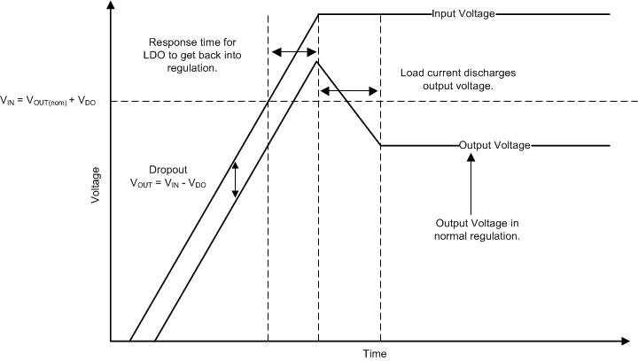
Some applications have transients that place the LDO into dropout, such as slower ramps on VIN during start-up. As with other LDOs, the output may overshoot on recovery from these conditions. A ramping input supply causes an LDO to overshoot on start-up, as shown in Figure 41, when the slew rate and voltage levels are in the correct range. Use an enable signal to avoid this condition.
 Figure 41. Startup Into Dropout
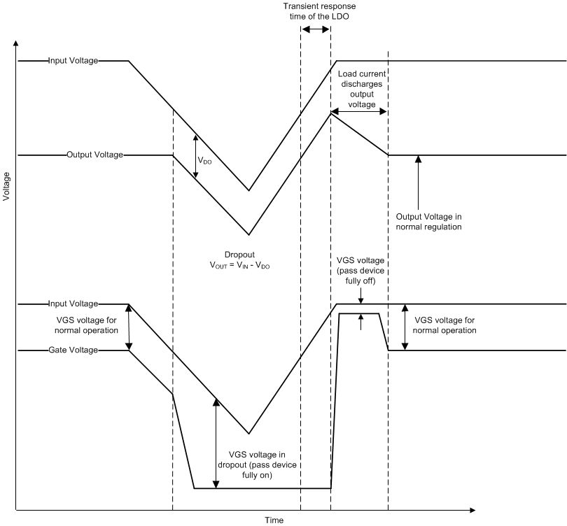
 Line transients out of dropout can also cause overshoot on the output of the regulator. These overshoots are caused by the error amplifier having to drive the gate capacitance of the pass element and bring the gate back to the correct voltage for proper regulation. Figure 42 illustrates what is happening internally with the gate voltage and how overshoot can be caused during operation. When the LDO is placed in dropout, the gate voltage (VGS) is pulled all the way down to ground to give the pass device the lowest on-resistance as possible. However, if a line transient occurs when the device is in dropout, the loop is not in regulation and can cause the output to overshoot until the loop responds and the output current pulls the output voltage back down into regulation. If these transients are not acceptable, then continue to add input capacitance in the system until the transient is slow enough to reduce the overshoot.
 Figure 42. Line Transients From Dropout