SBVS352A April   2018  – December 2018 TLV759P

PRODUCTION DATA.  

  1. Features
  2. Applications
  3. Description
    1.     Device Images
      1.      Typical Application
  4. Revision History
  5. Pin Configuration and Functions
    1.     Pin Functions
  6. Specifications
    1. 6.1 Absolute Maximum Ratings
    2. 6.2 ESD Ratings
    3. 6.3 Recommended Operating Conditions
    4. 6.4 Thermal Information
    5. 6.5 Electrical Characteristics
    6. 6.6 Typical Characteristics
  7. Detailed Description
    1. 7.1 Overview
    2. 7.2 Functional Block Diagram
    3. 7.3 Feature Description
      1. 7.3.1 Undervoltage Lockout (UVLO)
      2. 7.3.2 Shutdown
      3. 7.3.3 Foldback Current Limit
      4. 7.3.4 Thermal Shutdown
    4. 7.4 Device Functional Modes
      1. 7.4.1 Device Functional Mode Comparison
      2. 7.4.2 Normal Operation
      3. 7.4.3 Dropout Operation
      4. 7.4.4 Disabled
  8. Application and Implementation
    1. 8.1 Application Information
      1. 8.1.1 Adjustable Device Feedback Resistors
      2. 8.1.2 Input and Output Capacitor Selection
      3. 8.1.3 Dropout Voltage
      4. 8.1.4 Exiting Dropout
      5. 8.1.5 Reverse Current
      6. 8.1.6 Power Dissipation (PD)
    2. 8.2 Feed-Forward Capacitor (CFF)
    3. 8.3 Typical Application
      1. 8.3.1 Design Requirements
      2. 8.3.2 Detailed Design Procedure
        1. 8.3.2.1 Input Current
        2. 8.3.2.2 Thermal Dissipation
      3. 8.3.3 Application Curve
  9. Power Supply Recommendations
  10. 10Layout
    1. 10.1 Layout Guidelines
    2. 10.2 Layout Example
  11. 11Device and Documentation Support
    1. 11.1 Documentation Support
      1. 11.1.1 Related Documentation
    2. 11.2 Receiving Notification of Documentation Updates
    3. 11.3 Community Resources
    4. 11.4 Trademarks
    5. 11.5 Electrostatic Discharge Caution
    6. 11.6 Glossary
  12. 12Mechanical, Packaging, and Orderable Information

Package Options

Mechanical Data (Package|Pins)
Thermal pad, mechanical data (Package|Pins)
Orderable Information

Typical Characteristics

at operating temperature range TJ = 25°C, VIN = VOUT(NOM) + 0.5 V or 1.5 V (whichever is greater), IOUT = 1 mA, VEN = VIN, and CIN = COUT = 1 μF (unless otherwise noted)
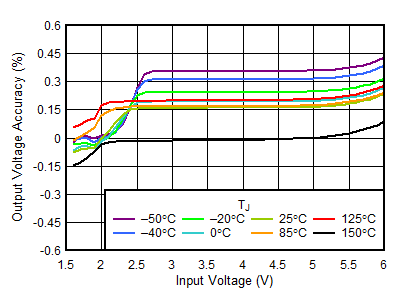
TLV759P D041-SBVS337.gif
VOUT = 3.3 V, IOUT = 1 mA
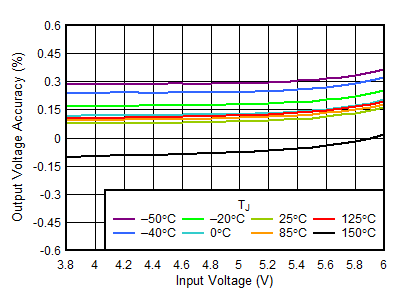
Figure 1. 3.3-V Line Regulation vs VIN
TLV759P D053-SBVS337.gif
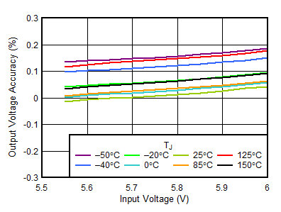
VOUT = 5.5 V, IOUT = 1 mA
Figure 3. 5.5-V Line Regulation vs VIN
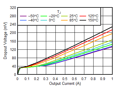
TLV759P D006-SBVS337.gif
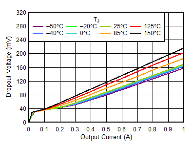
Figure 5. 0.55-V Dropout Voltage vs IOUT
TLV759P D021-SBVS337.gif
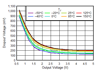
IOUT = 1 A
Figure 7. VDO vs VOUT
TLV759P D002-SBVS337.gif
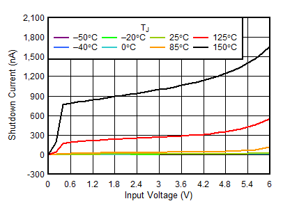
VEN = 0 V
Figure 9. ISHDN vs VIN
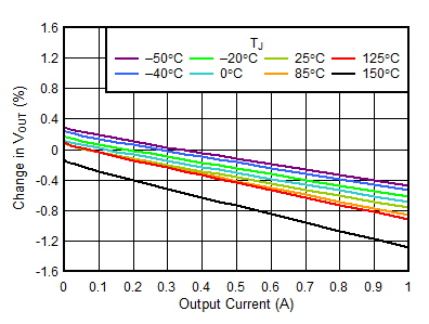
TLV759P D039-SBVS337.gif
VIN = 3.8 V, VOUT = 3.3 V
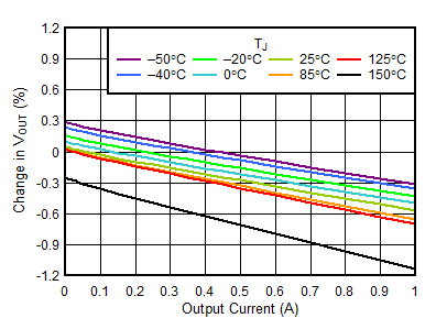
Figure 11. 3.3-V Load Regulation vs IOUT
TLV759P D055-SBVS337.gif
VIN = 6 V, VOUT = 5.5 V
Figure 13. 5-V Load Regulation vs IOUT
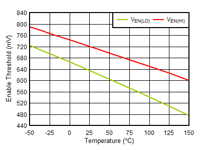
TLV759P D000-SBVS337.gif
Figure 15. VEN(HI) and VEN(LO) vs Temperature
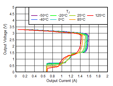
TLV759P D010-SBVS337.gif
Figure 17. 3.3-V Foldback Current Limit vs IOUT
TLV759P D012-SBVS337.gif
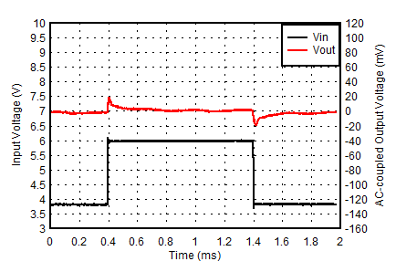
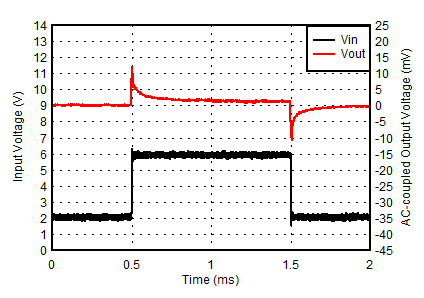
VOUT = 3.3 V, IOUT = 1 mA, VIN slew rate = 1 V/µs
Figure 19. 3.3-V Line Transient
TLV759P D014-SBVS337.gif
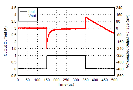
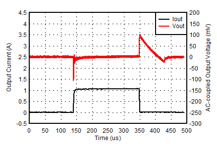
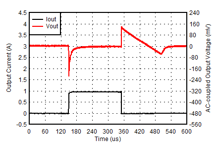
VOUT = 5 V, VIN = 5.5 V, IOUT slew rate = 1 A/µs
Figure 21. 1-mA to 1-A Load Transient (5 V)
TLV759P D016-SBVS337.gif
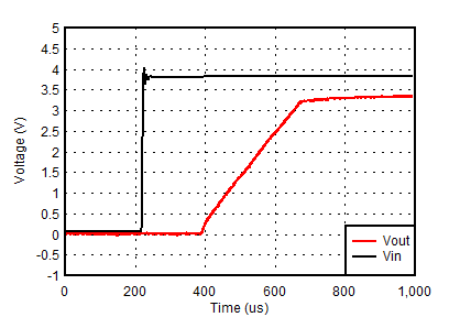
VIN = 3.8 V, VOUT = 3.3 V, IOUT = 1 mA
Figure 23. VIN Power-Up
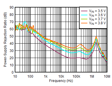
TLV759P D022-SBVS337.gif
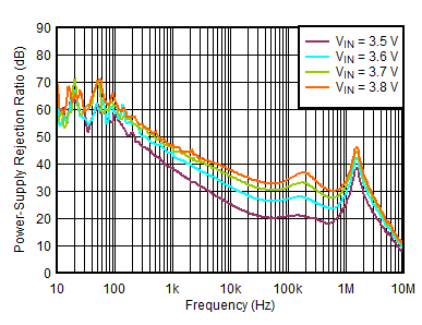
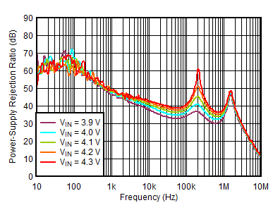
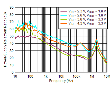
VOUT = 3.3 V, IOUT = 500 mA, COUT = 2.2 µF
Figure 25. PSRR vs Frequency and VIN
TLV759P D025-SBVS337.gif
VOUT = 3.3 V, IOUT = 250 mA, COUT = 2.2 µF
Figure 27. PSRR vs Frequency and VIN
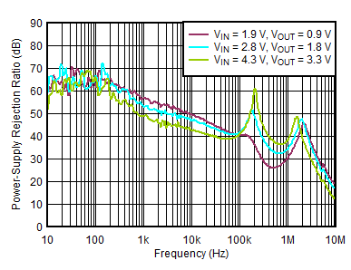
TLV759P D026-SBVS337.gif
IOUT = 500 mA, COUT = 2.2 µF
Figure 29. PSRR vs Frequency
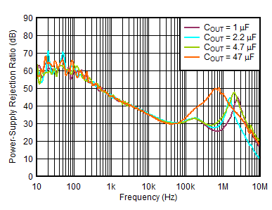
TLV759P D028-SBVS337.gif
VIN = 3.8 V, VOUT = 3.3 V, IOUT = 500 mA
Figure 31. PSRR vs Frequency and COUT
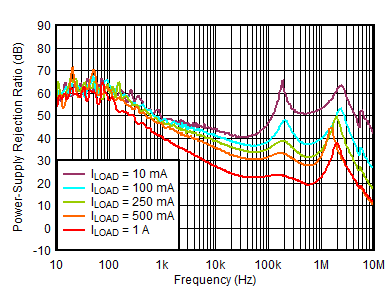
TLV759P D031-SBVS337.gif
VIN = 3.8 V, VOUT = 3.3 V, COUT = 2.2 µF
Figure 33. PSRR vs Frequency and ILOAD
TLV759P D033-SBVS337.gif
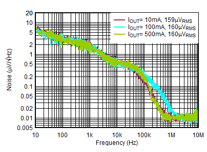
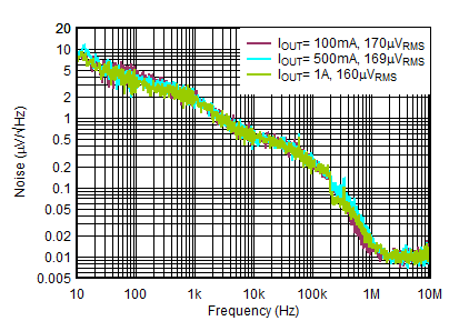
VIN = 3.8 V, VOUT = 3.3 V, COUT = 2.2 µF,
VRMS BW = 10 Hz to 100 kHz
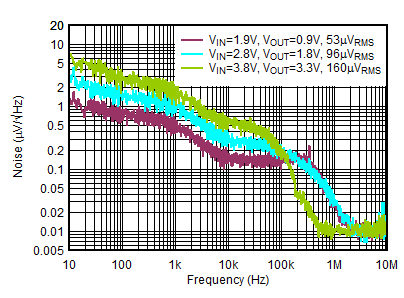
Figure 35. Output Spectral Noise Density
TLV759P D035-SBVS337.gif
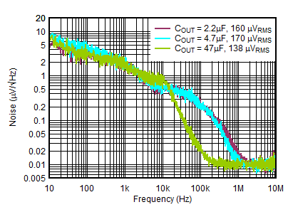
VIN = 3.8 V, VOUT = 3.3 V, IOUT = 100 mA, CFF = 0 µF,
VRMS BW = 10 Hz to 100 kHz
Figure 37. Output Spectral Noise Density vs
Frequency and COUT
TLV759P D004-SBVS337.gif
VOUT = 0.55 V, IOUT = 1 mA
Figure 2. 0.55-V Line Regulation vs VIN
TLV759P D038-SBVS337.gif
Figure 4. 3.3-V Dropout Voltage vs IOUT
TLV759P D051-SBVS337.gif
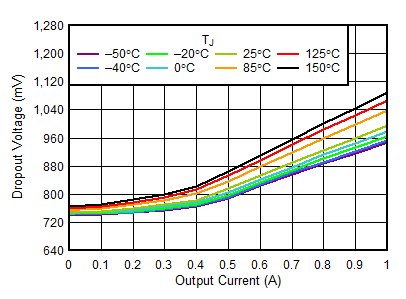
Figure 6. 5.5-V Dropout Voltage vs IOUT
TLV759P D008-SBVS337.gif
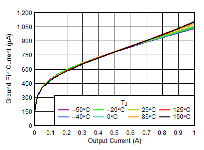
Figure 8. IGND vs IOUT
TLV759P D056-SBVS337.gif
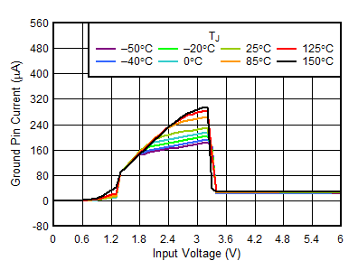
VOUT = 3.3 V, IOUT = 0 mA
Figure 10. IQ vs VIN
TLV759P D005-SBVS337.gif
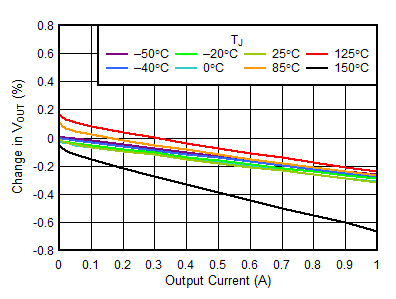
VIN = 2 V, VOUT = 0.55 V
Figure 12. 0.55-V Load Regulation vs IOUT
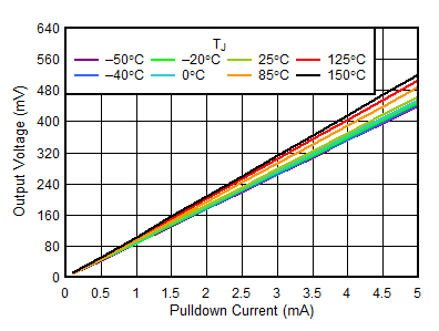
TLV759P D046-SBVS337.gif
Figure 14. VOUT vs IOUT Pulldown Resistor
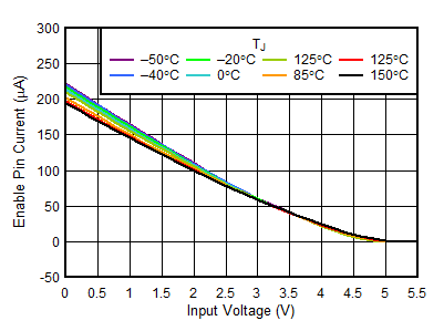
TLV759P D007-SBVS337.gif
VEN = 5.5 V
Figure 16. IEN vs VIN
TLV759P D011-SBVS337.gif
VOUT = 0.55 V, IOUT = 1 mA, VIN slew rate = 1 V/µs
Figure 18. 0.55-V Line Transient
TLV759P D013-SBVS337.gif
VOUT = 0.55 V, VIN = 2 V, IOUT slew rate = 1 A/µs
Figure 20. 1-mA to 1-A Load Transient (0.55 V)
TLV759P D015-SBVS337.gif
VOUT = 3.3 V, VIN = 3.8 V, IOUT slew rate = 1 A/µs
Figure 22. 1-mA to 1-A Load Transient (3.3 V)
TLV759P D018-SBVS337.gif
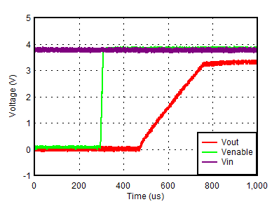
VIN = 3.8 V, VOUT = 3.3 V, IOUT = 1 mA
Figure 24. Startup With EN
TLV759P D023-SBVS337.gif
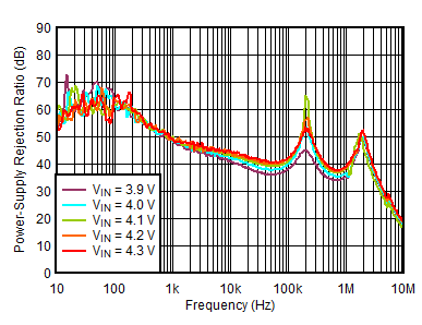
VOUT = 3.3 V, IOUT = 500 mA, COUT = 2.2 µF
Figure 26. PSRR vs Frequency and VIN
TLV759P D024-SBVS337.gif
VOUT = 3.3 V, IOUT = 250 mA, COUT = 2.2 µF
Figure 28. PSRR vs Frequency and VIN
TLV759P D027-SBVS337.gif
IOUT = 1 A, COUT = 2.2 µF
Figure 30. PSRR vs Frequency
TLV759P D029-SBVS337.gif
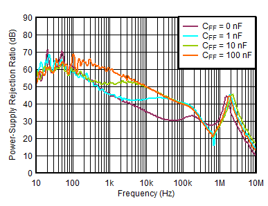
VIN = 3.8 V, VOUT = 3.3 V, IOUT = 500 mA
Figure 32. PSRR vs Frequency and CFF
TLV759P D032-SBVS337.gif
VIN = 3.8 V, VOUT = 3.3 V, COUT = 4.7 µF,
VRMS BW = 10 Hz to 100 kHz
Figure 34. Output Spectral Noise Density
TLV759P D034-SBVS337.gif
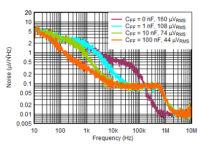
VIN = 3.8 V, VOUT = 3.3 V, IOUT = 500 mA, COUT = 2.2 µF,
VRMS BW = 10 Hz to 100 kHz
Figure 36. Output Spectral Noise Density vs
Frequency and CFF
TLV759P D042-SBVS337.gif
IOUT = 500 mA, COUT = 2.2 µF, VRMS BW = 10 Hz to 100 kHz
Figure 38. Output Spectral Noise Density vs Frequency