SBVS349C February   2020  – April 2024 TLV761

PRODMIX  

  1.   1
  2. Features
  3. Applications
  4. Description
  5. Pin Configuration and Functions
  6. Specifications
    1. 5.1 Absolute Maximum Ratings
    2. 5.2 ESD Ratings
    3. 5.3 Recommended Operating Conditions
    4. 5.4 Thermal Information
    5. 5.5 Electrical Characteristics
    6. 5.6 Typical Characteristics
  7. Detailed Description
    1. 6.1 Overview
    2. 6.2 Functional Block Diagram
    3. 6.3 Feature Description
      1. 6.3.1 Dropout Voltage
      2. 6.3.2 Foldback Current Limit
      3. 6.3.3 Undervoltage Lockout (UVLO)
      4. 6.3.4 Thermal Shutdown
    4. 6.4 Device Functional Modes
      1. 6.4.1 Device Functional Mode Comparison
      2. 6.4.2 Normal Operation
      3. 6.4.3 Dropout Operation
  8. Application and Implementation
    1. 7.1 Application Information
      1. 7.1.1 Recommended Capacitor Types
      2. 7.1.2 Input and Output Capacitor Requirements
      3. 7.1.3 Reverse Current
      4. 7.1.4 Power Dissipation (PD)
      5. 7.1.5 Estimating Junction Temperature
    2. 7.2 Typical Application
      1. 7.2.1 Design Requirements
      2. 7.2.2 Detailed Design Procedure
    3. 7.3 Best Design Practices
    4. 7.4 Power Supply Recommendations
    5. 7.5 Layout
      1. 7.5.1 Layout Guidelines
      2. 7.5.2 Layout Examples
  9. Device and Documentation Support
    1. 8.1 Device Support
      1. 8.1.1 Device Nomenclature
    2. 8.2 Documentation Support
      1. 8.2.1 Related Documentation
    3. 8.3 Receiving Notification of Documentation Updates
    4. 8.4 Support Resources
    5. 8.5 Trademarks
    6. 8.6 Electrostatic Discharge Caution
    7. 8.7 Glossary
  10. Revision History
  11. 10Mechanical, Packaging, and Orderable Information

Package Options

Mechanical Data (Package|Pins)
Thermal pad, mechanical data (Package|Pins)
Orderable Information

Typical Characteristics

at operating temperature TJ = 25°C, VIN = VOUT(NOM) + 1.5 V or 2.5 V (whichever is greater), IOUT = 10 mA, CIN = 1.0 µF, and COUT = 1.0 µF (unless otherwise noted)
GUID-B305DC2A-57D6-4082-801D-78B78DABB375-low.gif
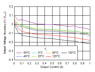
For VIN ≥ 3.0 V
Figure 5-1 VOUT Accuracy vs IOUT
GUID-DF2AECAB-3656-47C4-871A-8E706E7A5C80-low.gif
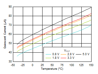
IOUT = 0 mA
Figure 5-3 IQ vs Temperature
GUID-3DFA72B7-27B8-4E36-BEB7-0A44D2277ACB-low.gif
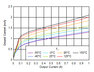
For VIN ≥ 3.0 V
Figure 5-5 IGND vs IOUT
GUID-DE96DD0C-4739-48C4-BE36-32C2968BB5E9-low.gif
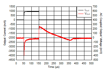
VIN = 5 V, VOUT = 3.3 V, ramp rate = 0.5 A/µs
Figure 5-7 IOUT Transient From 1 mA to 1 A
GUID-ABBC9EA3-00F8-47A4-BE32-6C2D44AF28D5-low.gif
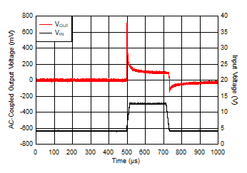
VIN = 5 V VOUT = 3.3 V, IOUT = 1 A, VIN ramp rate = 0.6 V/µs
Figure 5-9 VIN Transient in Dropout From 4 V to 13 V
GUID-1B9E8A48-6AC1-4BCD-9B52-1BFD77E866CE-low.gif
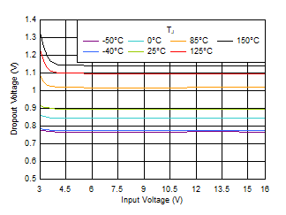
IOUT = 1.0 A
Figure 5-11 VDO vs VIN
GUID-DDFD9363-6993-48C6-A8E7-2A9CB5C9560D-low.gif
 
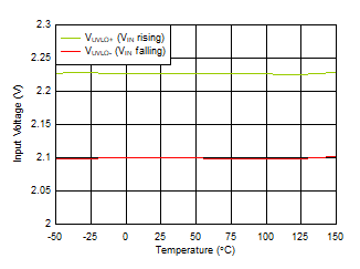
Figure 5-13 UVLO Thresholds vs Temperature
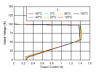
GUID-F504BA05-51D0-4B3B-94CD-494FD4D31BE6-low.gif
For VIN ≥ 3.0 V
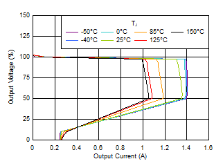
Figure 5-15 Foldback Current Limit vs Temperature
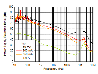
GUID-B01D42F9-6DF6-480F-A6CF-1715EA170EB6-low.gif
VOUT = 1.8 V, VIN = 3.3 V
Figure 5-17 PSRR vs IOUT
GUID-DCD44BDE-CD78-4921-BE0A-AB81D592D3EB-low.gif
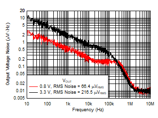
IOUT = 0.1 A, RMS noise BW = 10 Hz to 100 kHz
Figure 5-19 Output Noise (Vn) vs VOUT
GUID-A633FE3A-E44B-479A-B4F2-9765506A2E3A-low.gif
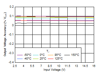
IOUT = 10 mA
Figure 5-2 VOUT Accuracy vs VIN
GUID-451BD5F2-6B62-4B50-A039-4E5D21AA7C07-low.gif
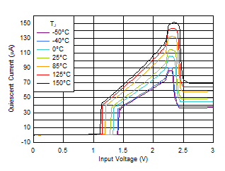
IOUT = 0 mA
Figure 5-4 IQ Increase Below Minimum VIN
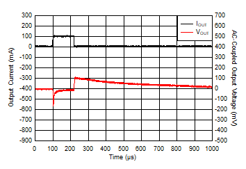
GUID-38D22332-D28C-4B0A-8503-C06ECFFDB44C-low.gif
VIN = 5 V, VOUT = 3.3 V, ramp rate = 0.4 A/µs
Figure 5-6 IOUT Transient From 0 mA to 100 mA
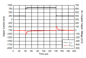
GUID-84A4F418-77AC-4CAB-BA76-78FCAF1D4A23-low.gif
VIN = 5 V, VOUT = 3.3 V, ramp rate = 0.8 A/µs
Figure 5-8 IOUT Transient From 250 mA to 850 mA
GUID-41CF0EAC-4BCA-4E27-9D2C-427B11356A9F-low.gif
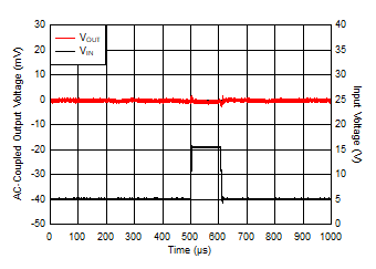
VOUT = 3.3 V, IOUT = 33 µA, VIN ramp rate = 1.6 V/µs
Figure 5-10 VIN Transient From 5 V to 16 V
GUID-BCE5BC73-F14B-4F3D-B6B4-8AC1DC3183CD-low.gif
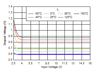
IOUT = 0.8 A
Figure 5-12 VDO vs VIN
GUID-8272B555-7B47-4AEA-91DB-EB5458390B9A-low.gif
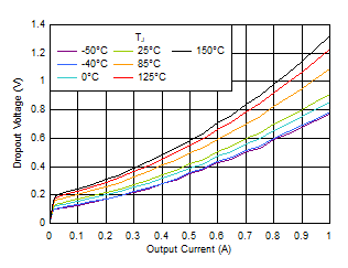
For VIN ≥ 3.0 V
Figure 5-14 VDO vs IOUT
GUID-0CD603BD-4374-41CD-8567-5BE375E46E05-low.gif
 
Figure 5-16 Foldback Current Limit vs Temperature
GUID-1952F316-717B-422F-BEC0-A95A5DD5E697-low.gif
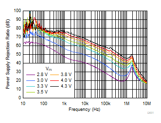
VOUT = 1.8 V, IOUT = 0.55 A
Figure 5-18 PSRR vs VIN
GUID-20221121-SS0I-ZGKW-STG5-XSXVTWKZGRLH-low.svg
IOUT = 0.1 A, COUT = 22 µF
Figure 5-20 Inrush Current With 22 µF at COUT