SBVS382A December   2020  – March 2023 TLV766-Q1

PRODUCTION DATA  

  1. Features
  2. Applications
  3. Description
  4. Revision History
  5. Pin Configuration and Functions
  6. Specifications
    1. 6.1 Absolute Maximum Ratings
    2. 6.2 ESD Ratings
    3. 6.3 Recommended Operating Conditions
    4. 6.4 Thermal Information
    5. 6.5 Electrical Characteristics
    6. 6.6 Typical Characteristics
  7. Detailed Description
    1. 7.1 Overview
    2. 7.2 Functional Block Diagrams
    3. 7.3 Feature Description
      1. 7.3.1 Output Enable
      2. 7.3.2 Dropout Voltage
      3. 7.3.3 Foldback Current Limit
      4. 7.3.4 Undervoltage Lockout (UVLO)
      5. 7.3.5 Output Pulldown
      6. 7.3.6 Thermal Shutdown
    4. 7.4 Device Functional Modes
      1. 7.4.1 Device Functional Mode Comparison
      2. 7.4.2 Normal Operation
      3. 7.4.3 Dropout Operation
      4. 7.4.4 Disabled
  8. Application and Implementation
    1. 8.1 Application Information
      1. 8.1.1 Adjustable Device Feedback Resistors
      2. 8.1.2 Recommended Capacitor Types
      3. 8.1.3 Input and Output Capacitor Requirements
      4. 8.1.4 Reverse Current
      5. 8.1.5 Feed-Forward Capacitor (CFF)
      6. 8.1.6 Power Dissipation (PD)
      7. 8.1.7 Estimating Junction Temperature
    2. 8.2 Typical Application
      1. 8.2.1 Design Requirements
      2. 8.2.2 Detailed Design Procedure
        1. 8.2.2.1 Transient Response
        2. 8.2.2.2 Choose Feedback Resistors
      3. 8.2.3 Application Curves
    3. 8.3 Power Supply Recommendations
    4. 8.4 Layout
      1. 8.4.1 Layout Guidelines
      2. 8.4.2 Layout Examples
  9. Device and Documentation Support
    1. 9.1 Device Support
      1. 9.1.1 Device Nomenclature
    2. 9.2 Documentation Support
      1. 9.2.1 Related Documentation
    3. 9.3 Receiving Notification of Documentation Updates
    4. 9.4 Support Resources
    5. 9.5 Trademarks
    6. 9.6 Electrostatic Discharge Caution
    7. 9.7 Glossary
  10. 10Mechanical, Packaging, and Orderable Information

Package Options

Mechanical Data (Package|Pins)
Thermal pad, mechanical data (Package|Pins)
Orderable Information

Application Curves

GUID-4707F463-308D-4F91-9FBE-650D02B0D9B2-low.gif
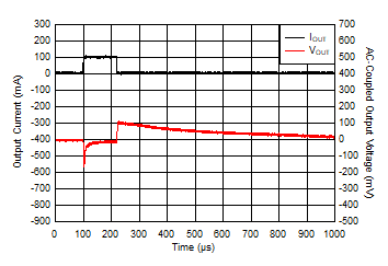
VIN = 5 V, VOUT = 3.3 V, COUT = 1 µF, CFF = 10 pF
Figure 8-3 Load Transient Response, IOUT 0 mA to 100 mA
GUID-863D3CCA-D1CA-47BE-9293-7504934E9FCA-low.gif
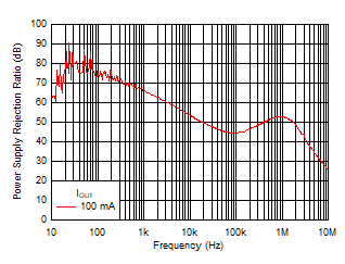
VIN = 5 V, VOUT = 3.3 V, COUT = 1 µF, CFF = 0 pF
Figure 8-4 PSRR Performance