SBVS381A April 2020 – December 2020 TLV767-Q1
PRODUCTION DATA
- 1 Features
- 2 Applications
- 3 Description
- 4 Revision History
- 5 Pin Configuration and Functions
- 6 Specifications
- 7 Detailed Description
- 8 Application and Implementation
- 9 Power Supply Recommendations
- 10Layout
- 11Device and Documentation Support
- 12Mechanical, Packaging, and Orderable Information
Package Options
Refer to the PDF data sheet for device specific package drawings
Mechanical Data (Package|Pins)
- DRB|8
Thermal pad, mechanical data (Package|Pins)
- DRB|8
Orderable Information
3 Description
The TLV767-Q1 is a wide input linear voltage regulator supporting an input voltage range from 2.5 V to 16 V and up to 1 A of load current. The output range is from 0.8 V to 12 V or up to 14.6 V with the adjustable version.
The wide input voltage range makes the device a good choice for operating from transformer secondary windings and regulated rails such as 10 V or 12 V. Additionally, the wide output voltage range allows the device to generate the bias voltage for silicon carbide (SiC) gate drivers and microphones as well as power microcontrollers (MCUs) and processors.
The TLV767-Q1 has a 1% output accuracy that is required for powering digital loads with tight supply requirements.
The internal soft-start circuit reduces inrush current during startup, thus allowing for smaller input capacitance.
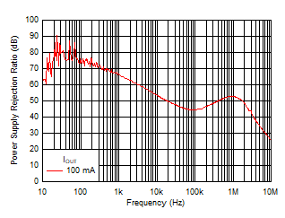
Wide bandwidth PSRR performance is greater than 70 dB at 1 kHz and 46 dB at 1 MHz, which helps attenuate the switching frequency of an upstream DC/DC converter and minimizes post regulator filtering. The high ripple rejection from 20 Hz to 20 kHz make the device a good choice for powering audio components.
The TLV767-Q1 is available in a 8-pin, 3-mm × 3-mm VSON (DRB) package with wettable flanks and low thermal resistance.
| PART NUMBER | PACKAGE | BODY SIZE (NOM) |
|---|---|---|
| TLV767-Q1 | VSON (8) | 3.00 mm × 3.00 mm |
 Typical Application
Circuit
 PSRR
Performance