SBVS453 May 2024 TLV770
PRODUCTION DATA
- 1
- 1 Features
- 2 Applications
- 3 Description
- 4 Pin Configuration and Functions
- 5 Specifications
- 6 Detailed Description
- 7 Application and Implementation
- 8 Device and Documentation Support
- 9 Revision History
- 10Mechanical, Packaging, and Orderable Information
Package Options
Refer to the PDF data sheet for device specific package drawings
Mechanical Data (Package|Pins)
- DBV|5
- DQN|4
Thermal pad, mechanical data (Package|Pins)
- DQN|4
Orderable Information
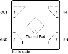
4 Pin Configuration and Functions
 Figure 4-1 DQN
Package,1mm × 1mm, 4-Pin
X2SON(Top View)
 Figure 4-2 DBV Package,5-Pin SOT-23(Top View)
Table 4-1 Pin Functions
| PIN | TYPE(1) | DESCRIPTION | ||
|---|---|---|---|---|
| NAME | X2SON | SOT-23 | ||
| EN | 3 | 3 | I | Enable input. A low voltage (< VEN(LOW)) on this pin turns the regulator off and discharges the output pin to GND. A high voltage (> VEN(HI)) on this pin enables the regulator output. |
| GND | 2 | 2 | G | Common ground. |
| IN | 4 | 1 | I | Input voltage supply. For best transient response and to minimize input impedance, use the nominal value or larger capacitor from IN to ground; see Section 5.3. Place the input capacitor as close to the IN and GND pins of the device as possible. |
| N/C | — | 4 | — | No internal electrical connection. Connect to GND for improved thermal performance. |
| OUT | 1 | 5 | O | Regulated output voltage. A low equivalent series resistance (ESR) capacitor is required from OUT to ground for stability. For best transient response, use the nominal recommended value or larger capacitor, as listed in Section 5.3. Place the output capacitor as close to the OUT and GND pins of the device as possible. An internal pulldown resistor prevents a charge from remaining on VOUT when the regulator is in shutdown mode (VEN< VEN(LOW)). |
| Thermal Pad | 5 | — | — | Thermal pad for the X2SON
package. Connect this pad to GND or leave floating. Do not connect to any potential other than GND. Connect the thermal pad to a large-area ground plane for best thermal performance. |
(1) I = input, O = output, I/O = input or output, and
G = ground.