SNOSD29E December   2016  – April 2018 TLV8541 , TLV8542 , TLV8544

UNLESS OTHERWISE NOTED, this document contains PRODUCTION DATA.  

  1. Features
  2. Applications
  3. Description
    1.     Device Images
      1.      Low Power PIR Motion Detector
  4. Revision History
  5. Description (continued)
  6. Pin Configuration and Functions
    1.     Pin Functions: TLV8541 DBV
    2.     Pin Functions: TLV8542 D & RUG
    3.     Pin Functions: TLV8544 PW & D
  7. Specifications
    1. 7.1 Absolute Maximum Ratings
    2. 7.2 ESD Ratings
    3. 7.3 Recommended Operating Conditions
    4. 7.4 Thermal Information
    5. 7.5 Electrical Characteristics
    6. 7.6 Typical Characteristics
  8. Detailed Description
    1. 8.1 Overview
    2. 8.2 Functional Block Diagram
    3. 8.3 Feature Description
    4. 8.4 Device Functional Modes
      1. 8.4.1 Rail-To-Rail Input
      2. 8.4.2 Supply Current Changes Over Common Mode
      3. 8.4.3 Design Optimization With Rail-To-Rail Input
      4. 8.4.4 Design Optimization for Nanopower Operation
      5. 8.4.5 Common-Mode Rejection
      6. 8.4.6 Output Stage
      7. 8.4.7 Driving Capacitive Load
  9. Application and Implementation
    1. 9.1 Application Information
    2. 9.2 Typical Application: Battery-Powered Wireless PIR Motion Detectors
      1. 9.2.1 Design Requirements
      2. 9.2.2 Detailed Design Procedure
        1. 9.2.2.1 Calculation of the Cutoff Frequencies and Gain of Stage A:
        2. 9.2.2.2 Calculation of the Cutoff Frequencies and Gain of Stage B
        3. 9.2.2.3 Calculation of the Total Gain of Stages A and B
        4. 9.2.2.4 Window Comparator Stage
        5. 9.2.2.5 Reference Voltages
      3. 9.2.3 Application Curve
    3. 9.3 Typical Application: 60-Hz Twin T Notch Filter
      1. 9.3.1 Design Requirements
      2. 9.3.2 Detailed Design Procedure
      3. 9.3.3 Application Curve
    4. 9.4 Dos and Don'ts
  10. 10Power Supply Recommendations
  11. 11Layout
    1. 11.1 Layout Guidelines
    2. 11.2 Layout Example
  12. 12Device and Documentation Support
    1. 12.1 Device Support
      1. 12.1.1 Development Support
    2. 12.2 Documentation Support
      1. 12.2.1 Related Documentation
    3. 12.3 Related Links
    4. 12.4 Receiving Notification of Documentation Updates
    5. 12.5 Community Resources
    6. 12.6 Trademarks
    7. 12.7 Electrostatic Discharge Caution
    8. 12.8 Glossary
  13. 13Mechanical, Packaging, and Orderable Information

Package Options

Mechanical Data (Package|Pins)
Thermal pad, mechanical data (Package|Pins)
Orderable Information

Typical Characteristics

TA = 25°C, RL = 10 MΩ to VS/2 ,CL = 20 pF, VCM = VS / 2 V unless otherwise specified.
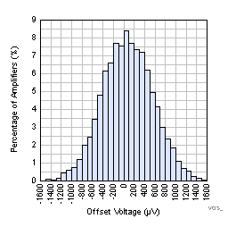
TLV8544 TLV8542 TLV8541 VOS_HSTG_1p8_VP.gif
VS = 1.8 V VCM = V+ Data from 1500 4-channel devices
Figure 1. Offset Voltage Production Distribution
TLV8544 TLV8542 TLV8541 VOS_HSTG_3p3_VP.gif
VS = 3.3 V VCM = V+ Data from 1500 4-channel devices
Figure 3. Offset Voltage Production Distribution
TLV8544 TLV8542 TLV8541 SNOSD29_IQ_Vs_Vcm_1p8V_3Temp.gif
VS = 1.8 V TA = –40, 25, 125°C Per Channel
Figure 5. Supply Current vs Common Mode Voltage
TLV8544 TLV8542 TLV8541 Vos-vs-Vcm-3T-Vs1p8V-Tim.gif
VS = 1.8 V TA = –40, 25, 125°C
Figure 7. Typical Offset Voltage vs Common Mode Voltage
TLV8544 TLV8542 TLV8541 SNOSD29_IQ_Vs_Vs_3Temp_FNL_PCK.gif
VS = 1.6 to 3.6V TA = –40, 25, 125°C VCM = V-
Figure 9. Supply Current vs Supply Voltage, Low VCM
TLV8544 TLV8542 TLV8541 PSRR_vs_Freq_SNOSD29.gif
VS= 3.3V TA = 25°C VCM = V–
Figure 11. PSRR vs Frequency
TLV8544 TLV8542 TLV8541 SNOSD29_Output_Swing_Vs_Isink_3p3VS.gif
VS = 3.3 V TA = –40, 25, 125°C
Figure 13. Output Swing vs Sinking Current
TLV8544 TLV8542 TLV8541 SNOSD29_Output_Swing_Vs_Isource_3p3VS.gif
VS = 3.3 V TA = –40, 25, 125°C
Figure 15. Output Swing vs Sourcing Current
TLV8544 TLV8542 TLV8541 SNOSD29_Ibias_Vcm_3p3_M40C.gif
VS = 3.3 V TA = –40°C
Figure 17. Input Bias Current vs Common Mode Voltage
TLV8544 TLV8542 TLV8541 SNOSD29_Ibias_Vcm_3p3_25C.gif
VS = 3.3 V TA = 25°C
Figure 19. Input Bias Current vs Common Mode Voltage
TLV8544 TLV8542 TLV8541 SNOSD29_Ibias_vs_Vcm_125C_3.3V.gif
VS = 3.3 V TA = 125°C
Figure 21. Input Bias Current vs Common Mode Voltage
TLV8544 TLV8542 TLV8541 SNOSD29_Noise_Vol_Dens_Vs_Freq.gif
VS = 3.3 V TA = 25°C
Figure 23. Input Voltage Noise vs Frequency
TLV8544 TLV8542 TLV8541 SNOSD29_EMIRR.gif
VS = 3.3 V TA = 25°C
AV = 1
Figure 25. EMIRR Performance
TLV8544 TLV8542 TLV8541 SNOSD29_Step_RES_3p3Vs_0p2Vp-pVin.gif
VS = 3.3 V TA = 25 °C CL = 50 pF
VIN = 1.65 ± 0.1 V AV = 1
Figure 27. Small Signal Pulse Response, 3.3 V
TLV8544 TLV8542 TLV8541 SNOSD29_Step_RES_3p3Vs_2Vp-pVin.gif
VS = 3.3 V TA = 25°C CL = 50 pF
VIN = 1.65 ± 1 V AV = 1
Figure 29. Large Signal Pulse Response, 3.3 V
TLV8544 TLV8542 TLV8541 VOS_HSTG_1p8_VM.gif
VS = 1.8 V VCM = V– Data from 1500 4-channel devices
Figure 2. Offset Voltage Production Distribution
TLV8544 TLV8542 TLV8541 VOS_HSTG_3p3_VM.gif
VS = 3.3 V VCM = V– Data from 1500 4-channel devices
Figure 4. Offset Voltage Production Distribution
TLV8544 TLV8542 TLV8541 SNOSD29_IQ_Vs_Vcm_3p3V_3Temp.gif
VS = 3.3 V TA = –40, 25, 125°C Per Channel
Figure 6. Supply Current vs Common Mode Voltage
TLV8544 TLV8542 TLV8541 Vos-vs-Vcm-3T-Vs3p3V-Tim.gif
VS = 3.3 V TA = –40, 25, 125°C
Figure 8. Typical Offset Voltage vs Common Mode Voltage
TLV8544 TLV8542 TLV8541 SNOSD29_CMRR_vs_Frequncy.gif
VS= 3.3V TA = 25°C
Figure 10. CMRR vs Frequency
TLV8544 TLV8542 TLV8541 SNOSD29_Output_Swing_Vs_Isink_1p8VS.gif
VS = 1.8 V TA = –40, 25, 125°C
Figure 12. Output Swing vs Sinking Current
TLV8544 TLV8542 TLV8541 SNOSD29_Output_Swing_Vs_Isource_1p8VS.gif
VS = 1.8 V TA = –40, 25, 125°C
Figure 14. Output Swing vs Sourcing Current
TLV8544 TLV8542 TLV8541 SNOSD29_Ibias_vs_Vcm_M40C_1p8.gif
VS = 1.8 V TA = –40°C
Figure 16. Input Bias Current vs Common Mode Voltage
TLV8544 TLV8542 TLV8541 SNOSD29_Ibias_Vcm_1p8_25C.gif
VS = 1.8 V TA = 25°C
Figure 18. Input Bias Current vs Common Mode Voltage
TLV8544 TLV8542 TLV8541 SNOSD29_Ibias_Vcm_1p8_125C.gif
VS= 1.8V TA = 125°C
Figure 20. Input Bias Current vs Common Mode Voltage
TLV8544 TLV8542 TLV8541 AOL_vs_fre_tritemp.gif
VS = 3.3 V TA = –40, 25, 125°C CL = 50 pF
Figure 22. Open Loop Gain and Phase
TLV8544 TLV8542 TLV8541 SNOSD29_ZO_Vs_Feq_3p3VS.gif
VS = 3.3 V TA = 25°C
Figure 24. Open Loop Output Impedance
TLV8544 TLV8542 TLV8541 SNOSD29_Step_RES_1p8Vs_0p2Vp-pVin.gif
VS = 1.8 V TA = 25°C CL = 50 pF
VIN = 0.9 ± 0.1 V AV = 1
Figure 26. Small Signal Pulse Response, 1.8 V
TLV8544 TLV8542 TLV8541 SNOSD29_Step_RES_1p8Vs_1Vp-pVin.gif
VS = 1.8 V TA = 25°C CL = 50 pF
VIN = 0.9 ± 0.5 V AV = 1
Figure 28. Large Signal Pulse Response, 1.8 V