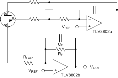
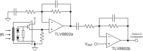
The TLV8801 (single) and TLV8802 (dual) family of ultra-low-power operational amplifiers are ideal for cost-optimized sensing applications in wireless and low power wired equipment. The TLV880x amplifiers minimize power consumption in equipment such as CO detectors, smoke detectors and motion detecting security systems (like PIR motion sensing) where operational battery-life is critical. They also have a carefully designed CMOS input stage enabling very low, femto-amp bias currents, thereby reducing IBIAS and IOS errors that would otherwise impact sensitive applications like transimpedance amplifier (TIA) configurations with megaohm feedback resistors, and high source impedance sensing applications. Additionally, built-in EMI protection reduces sensitivity to unwanted RF signals from sources like mobile phones, WiFi, radio transmitters and tag readers.
The TLV8801 (single) and TLV8802 (dual) channel versions are available in industry standard 5-pin SOT-23 and 8-pin VSSOP packages respectively.
PART NUMBER | CHANNELS | SUPPLY CURRENT (Typ/Ch) | OFFSET VOLTAGE (Max) |
---|---|---|---|
TLV8801 | 1 | 450 nA | 4.5 mV |
TLV8802 | 2 | 320 nA | 4.5 mV |
LPV801 | 1 | 450 nA | 3.5 mV |
LPV802 | 2 | 320 nA | 3.5 mV |
PART NUMBER | PACKAGE | BODY SIZE |
---|---|---|
TLV8801 | SOT-23 (5) | 2.90 mm x 1.60 mm |
TLV8802 | VSSOP (8) | 3.00 mm × 3.00 mm |
PIN | I/O | DESCRIPTION | ||
---|---|---|---|---|
NAME | NUMBER | |||
OUT | 1 | O | Output | |
-IN | 4 | I | Inverting Input | |
+IN | 3 | I | Non-Inverting Input | |
V- | 2 | P | Negative (lowest) power supply | |
V+ | 5 | P | Positive (highest) power supply |
PIN | I/O | DESCRIPTION | ||
---|---|---|---|---|
NAME | NUMBER | |||
OUT A | 1 | O | Channel A Output | |
-IN A | 2 | I | Channel A Inverting Input | |
+IN A | 3 | I | Channel A Non-Inverting Input | |
V- | 4 | P | Negative (lowest) power supply | |
+IN B | 5 | I | Channel B Non-Inverting Input | |
-IN B | 6 | I | Channel B Inverting Input | |
OUT B | 7 | O | Channel B Output | |
V+ | 8 | P | Positive (highest) power supply |
MIN | MAX | UNIT | |||
---|---|---|---|---|---|
Supply voltage, Vs = (V+) - (V-) | –0.3 | 6 | V | ||
Input pins | Voltage (2) (3) | Common mode | (V-) - 0.3 | (V+) + 0.3 | V |
Differential | (V-) - 0.3 | (V+) + 0.3 | V | ||
Input pins | Current | -10 | 10 | mA | |
Output short current (4) | Continuous | Continuous | |||
Storage temperature, Tstg | –65 | 150 | °C | ||
Junction temperature | 150 | °C |
VALUE | UNIT | |||
---|---|---|---|---|
V(ESD) | Electrostatic discharge | Human-body model (HBM), per ANSI/ESDA/JEDEC JS-001(1) | ±1000 | V |
Charged-device model (CDM), per JEDEC specification JESD22-C101(2) | ±250 |
MIN | NOM | MAX | UNIT | ||
---|---|---|---|---|---|
Supply voltage (V+ – V–) | 1.7 | 5.5 | V | ||
Specified temperature | -40 | 125 | °C |
THERMAL METRIC(1) | TLV8801 DBV 5 PINS | TLV8802 DGK 8 PINS | UNIT | |
---|---|---|---|---|
θJA | Junction-to-ambient thermal resistance | 177.4 | 177.6 | ºC/W |
θJCtop | Junction-to-case (top) thermal resistance | 133.9 | 68.8 | |
θJB | Junction-to-board thermal resistance | 36.3 | 98.2 | |
ψJT | Junction-to-top characterization parameter | 23.6 | 12.3 | |
ψJB | Junction-to-board characterization parameter | 35.7 | 96.7 |
VCM = V- | TLV8801 | RL=No Load |
VS= 1.8V | RL= 10MΩ |
VS= 5V | RL= 10MΩ |
VS= 1.8V | TA = -40°C |
VS= 1.8V | TA = 25°C |
VS= 1.8V | TA = 125°C |
VS= 1.8V | RL= No Load |
VS= 3.3V | RL= No Load |
VS= 5V | RL= No Load |
TA = 25 | RL= 10MΩ | Vout = 200mVpp |
VS= ±0.9V | CL= 20pF | AV = +1 |
TA = 25 | RL= 10MΩ | Vout = 1Vpp |
VS= ±0.9V | CL= 20pF | AV = +1 |
TA = 25 | RL= 10MΩ | ΔVCM = 0.5Vpp |
VS= 5V | CL= 20p | |
VCM = Vs/2 | AV = +1 |
TA = -40, 25, 125°C | RL= 10MΩ | VOUT = 200mVPP |
VS= 5V | CL= 20pF | VCM = Vs/2 |
TA = -40, 25, 125°C | RL= 1MΩ | VOUT = 200mVPP |
VS= 5V | CL= 20pF | VCM = Vs/2 |
TA = -40, 25, 125°C | RL= 100kΩ | VOUT = 200mVPP |
VS= 5V | CL= 20pF | VCM = Vs/2 |
TA = -40, 25, 125°C | RL= 10MΩ | VOUT = 200mVPP |
VS= 1.8V | CL= 20pF | VCM = Vs/2 |
TA = -40, 25, 125°C | RL= 1MΩ | VOUT = 200mVPP |
VS= 1.8V | CL= 20pF | VCM = Vs/2 |
TA = -40, 25, 125°C | RL= 100kΩ | VOUT = 200mVPP |
VS= 1.8V | CL= 20pF | VCM = Vs/2 |
VCM = V- | TLV8802 | RL=No Load |
VS= 3.3V | RL= 10MΩ |
VS= 5V | TA = -40 to 125 | VCM = Vs/2 |
VS= 5V | TA = -40°C |
VS= 5V | TA = 25°C |
VS= 5V | TA = 125°C |
VS= 1.8V | RL= No Load |
VS= 3.3V | RL= No Load |
VS= 5V | RL= No Load |
TA = 25 | RL= 10MΩ | Vout = 200mVpp |
VS= ±2.5V | CL= 20pF | AV = +1 |
TA = 25 | RL= 10MΩ | Vout = 2Vpp |
VS= ±2.5V | CL= 20pF | AV = +1 |
TA = 25 | RL= 10MΩ | ΔVS = 0.5Vpp |
VS= 3.3V | CL= 20p | |
VCM = Vs/2 | AV = +1 |
TA = -40, 25, 125°C | RL= 10MΩ | VOUT = 200mVPP |
VS= 3.3V | CL= 20pF | VCM = Vs/2 |
TA = -40, 25, 125°C | RL= 1MΩ | VOUT = 200mVPP |
VS= 3.3V | CL= 20pF | VCM = Vs/2 |
TA = -40, 25, 125°C | RL= 100kΩ | VOUT = 200mVPP |
VS= 3.3V | CL= 20pF | VCM = Vs/2 |
TA = 25°C | VS= 5 V | RL= 10MΩ |
TA = 25 | RL= 1MΩ | VCM = Vs/2 |
VS= 5V | CL= 20pF | AV = +1 |
TA = 25 | RL= 1MΩ | VCM = Vs/2 |
VS= 3.3V | CL= 20pF | AV = +1 |
The TLV8801 (single) and TLV8802 (dual) series nanoPower CMOS operational amplifiers are designed for long-life battery-powered and energy harvested applications. They operate on a single supply with operation as low as 1.7 V. The output is rail-to-rail and swings to within 3.5mV of the supplies with a 100kΩ load. The common-mode range extends to the negative supply making it ideal for single-supply applications. EMI protection has been employed internally to reduce the effects of EMI.
Parameters that vary significantly with operating voltages or temperature are shown in the Typical Characteristics curves.
The amplifier's differential inputs consist of a non-inverting input (+IN) and an inverting input (–IN). The amplifer amplifies only the difference in voltage between the two inputs, which is called the differential input voltage. The output voltage of the op-amp VOUT is given by Equation 1:
where
The input common-mode voltage range of the TLV880x extends from (V-) to (V+) – 0.9 V. In this range, low offset can be expected with a minimum of 80dB CMRR. The TLV880x is protected from output "inversions" or "reversals".
The TLV880x output voltage swings 3.5 mV from rails at 1.8 V supply, which provides the maximum possible dynamic range at the output. This is particularly important when operating on low supply voltages.
The TLV880x Maximum Output Voltage Swing graph defines the maximum swing possible under a particular output load.
When designing for ultralow power, choose system feedback components carefully. To minimize quiecent current consumption, select large-value feedback resistors. Any large resistors will react with stray capacitance in the circuit and the input capacitance of the operational amplifier. These parasitic RC combinations can affect the stability of the overall system. A feedback capacitor may be required to assure stability and limit overshoot or gain peaking.
When possible, use AC coupling and AC feedback to reduce static current draw through the feedback elements. Use film or ceramic capacitors since large electolytics may have large static leakage currents in the nanoamps.
The TLV880x is internally compensated for stable unity gain operation, with a 6 kHz typical gain bandwidth. However, the unity gain follower is the most sensitive configuration to capacitive load. The combination of a capacitive load placed directly on the output of an amplifier along with the amplifier’s output impedance creates a phase lag, which reduces the phase margin of the amplifier. If the phase margin is significantly reduced, the response will be under damped which causes peaking in the transfer and, when there is too much peaking, the op amp might start oscillating.
In order to drive heavy (>50pF) capacitive loads, an isolation resistor, RISO, should be used, as shown in Figure 37. By using this isolation resistor, the capacitive load is isolated from the amplifier’s output. The larger the value of RISO, the more stable the amplifier will be. If the value of RISO is sufficiently large, the feedback loop will be stable, independent of the value of CL. However, larger values of RISO result in reduced output swing and reduced output current drive. The recommended value for RISO is 30-50kΩ.
NOTE
Information in the following applications sections is not part of the TI component specification, and TI does not warrant its accuracy or completeness. TI’s customers are responsible for determining suitability of components for their purposes. Customers should validate and test their design implementation to confirm system functionality.
The TLV880x is a ultra-low power operational amplifier that provides 6 kHz bandwidth with only 320nA typical quiescent current, and near precision drift specifications. These rail-to-rail output amplifiers are specifically designed for battery-powered applications. The input common-mode voltage range extends to the negative supply rail and the output swings to within millivolts of the rails, maintaining a wide dynamic range.
Figure 38 shows a simple micropower potentiostat circuit for use with three terminal unbiased CO sensors, though it is applicable to many other type of three terminal gas sensors or electrochemical cells.
The basic sensor has three electrodes; The Sense or Working Electrode (“WE”), Counter Electrode (“CE”) and Reference Electrode (“RE”). A current flows between the CE and WE proportional to the detected concentration.
The RE monitors the potential of the internal reference point. For an unbiased sensor, the WE and RE electrodes must be maintained at the same potential by adjusting the bias on CE. Through the Potentiostat circuit formed by U1, the servo feedback action will maintain the RE pin at a potential set by VREF.
R1 is to maintain stability due to the large capacitance of the sensor. C1 and R2 form the Potentiostat integrator and set the feedback time constant.
U2 forms a transimpedance amplifier ("TIA") to convert the resulting sensor current into a proportional voltage. The transimpedance gain, and resulting sensitivity, is set by RF according to Equation 2.
RL is a load resistor of which the value is normally specified by the sensor manufacturer (typically 10 ohms). The potential at WE is set by the applied VREF. Riso provides capacitive isolation and, combined with C2, form the output filter and ADC reservoir capacitor to drive the ADC.
For this example, we will be using a CO sensor with a sensitivity of 69nA/ppm. The supply votlage and maximum ADC input voltage is 2.5V, and the maximum concentration is 300ppm.
First the VREF voltage must be determined. This voltage is a compromise between maximum headroom and resolution, as well as allowance for "footroom" for the minimum swing on the CE terminal, since the CE terminal generally goes negative in relation to the RE potential as the concentration (sensor current) increases. Bench measurements found the difference between CE and RE to be 180mV at 300ppm for this particular sensor.
To allow for negative CE swing "footroom" and voltage drop across the 10k resistor, 300mV was chosen for VREF.
Therefore +300mV will be used as the minimum VZERO to add some headroom.
where
Next we calculate the maximum sensor current at highest expected concentration:
where
Now find the available output swing range above the reference voltage available for the measurement:
where
Now we calculate the transimpedance resistor (RF) value using the maximum swing and the maximum sensor current:
Figure 39 shows the resulting circuit voltages when the sensor was exposed to 200ppm step of carbon monoxide gas. VC is the monitored CE pin voltage and clearly shows the expected CE voltage dropping below the WE voltage, VW, as the concentration increases.
VTIA is the output of the transimpedance amplifer U2. VDIFF is the calculated difference between VREF and VTIA, which will be used for the ppm calculation.
Figure 40 shows the calculated sensor current using the formula in Equation 7 :
Equation 8 shows the resulting conversion of the sensor current into ppm.
Total supply current for the amplifier section is less than 700 nA, minus sensor current. Note that the sensor current is sourced from the amplifier output, which in turn comes from the amplifier supply voltage. Therefore, any continuous sensor current must also be included in supply current budget calculations.
Do properly bypass the power supplies.
Do add series resistance to the output when driving capacitive loads, particularly cables, Muxes and ADC inputs.
Do add series current limiting resistors and external schottky clamp diodes if input voltage is expected to exceed the supplies. Limit the current to 1mA or less (1KΩ per volt).
The TLV880x is specified for operation from 1.7 V to 5.5 V (±0.75 V to ±2.75 V) over a –40°C to 125°C temperature range. Parameters that can exhibit significant variance with regard to operating voltage or temperature are presented in the Typical Characteristics.
CAUTION
Supply voltages larger than 6 V can permanently damage the device.
For proper operation, the power supplies must be properly decoupled. For decoupling the supply lines it is suggested that 100 nF capacitors be placed as close as possible to the operational amplifier power supply pins. For single supply, place a capacitor between V+ and V– supply leads. For dual supplies, place one capacitor between V+ and ground, and one capacitor between V– and ground.
Low bandwidth nanopower devices do not have good high frequency (> 1 kHz) AC PSRR rejection against high-frequency switching supplies and other 1 kHz and above noise sources, so extra supply filtering is recommended if kilohertz or above noise is expected on the power supply lines.
The V+ pin should be bypassed to ground with a low ESR capacitor.
The optimum placement is closest to the V+ and ground pins.
Care should be taken to minimize the loop area formed by the bypass capacitor connection between V+ and ground.
The ground pin should be connected to the PCB ground plane at the pin of the device.
The feedback components should be placed as close to the device as possible to minimize strays.
TINA-TI SPICE-Based Analog Simulation Program, http://www.ti.com/tool/tina-ti
DIP Adapter Evaluation Module, http://www.ti.com/tool/dip-adapter-evm
TI Universal Operational Amplifier Evaluation Module, http://www.ti.com/tool/opampevm
TI FilterPro Filter Design software, http://www.ti.com/tool/filterpro
The table below lists quick access links. Categories include technical documents, support and community resources, tools and software, and quick access to sample or buy.
PARTS | PRODUCT FOLDER | SAMPLE & BUY | TECHNICAL DOCUMENTS | TOOLS & SOFTWARE | SUPPORT & COMMUNITY |
---|---|---|---|---|---|
TLV8801 | Click here | Click here | Click here | Click here | Click here |
TLV8802 | Click here | Click here | Click here | Click here | Click here |
To receive notification of documentation updates, navigate to the device product folder on ti.com. In the upper right corner, click on Alert me to register and receive a weekly digest of any product information that has changed. For change details, review the revision history included in any revised document.
The following links connect to TI community resources. Linked contents are provided "AS IS" by the respective contributors. They do not constitute TI specifications and do not necessarily reflect TI's views; see TI's Terms of Use.
E2E is a trademark of Texas Instruments.
All other trademarks are the property of their respective owners.
These devices have limited built-in ESD protection. The leads should be shorted together or the device placed in conductive foam during storage or handling to prevent electrostatic damage to the MOS gates.
SLYZ022 — TI Glossary.
This glossary lists and explains terms, acronyms, and definitions.
The following pages include mechanical, packaging, and orderable information. This information is the most current data available for the designated devices. This data is subject to change without notice and revision of this document. For browser-based versions of this data sheet, refer to the left-hand navigation.
Texas Instruments Incorporated and its subsidiaries (TI) reserve the right to make corrections, enhancements, improvements and other changes to its semiconductor products and services per JESD46, latest issue, and to discontinue any product or service per JESD48, latest issue. Buyers should obtain the latest relevant information before placing orders and should verify that such information is current and complete. All semiconductor products (also referred to herein as "components") are sold subject to TI's terms and conditions of sale supplied at the time of order acknowledgment.
TI warrants performance of its components to the specifications applicable at the time of sale, in accordance with the warranty in TI's terms and conditions of sale of semiconductor products. Testing and other quality control techniques are used to the extent TI deems necessary to support this warranty. Except where mandated by applicable law, testing of all parameters of each component is not necessarily performed.
TI assumes no liability for applications assistance or the design of Buyers' products. Buyers are responsible for their products and applications using TI components. To minimize the risks associated with Buyers' products and applications, Buyers should provide adequate design and operating safeguards.
TI does not warrant or represent that any license, either express or implied, is granted under any patent right, copyright, mask work right, or other intellectual property right relating to any combination, machine, or process in which TI components or services are used. Information published by TI regarding third-party products or services does not constitute a license to use such products or services or a warranty or endorsement thereof. Use of such information may require a license from a third party under the patents or other intellectual property of the third party, or a license from TI under the patents or other intellectual property of TI.
Reproduction of significant portions of TI information in TI data books or data sheets is permissible only if reproduction is without alteration and is accompanied by all associated warranties, conditions, limitations, and notices. TI is not responsible or liable for such altered documentation. Information of third parties may be subject to additional restrictions.
Resale of TI components or services with statements different from or beyond the parameters stated by TI for that component or service voids all express and any implied warranties for the associated TI component or service and is an unfair and deceptive business practice. TI is not responsible or liable for any such statements.
Buyer acknowledges and agrees that it is solely responsible for compliance with all legal, regulatory and safety-related requirements concerning its products, and any use of TI components in its applications, notwithstanding any applications-related information or support that may be provided by TI. Buyer represents and agrees that it has all the necessary expertise to create and implement safeguards which anticipate dangerous consequences of failures, monitor failures and their consequences, lessen the likelihood of failures that might cause harm and take appropriate remedial actions. Buyer will fully indemnify TI and its representatives against any damages arising out of the use of any TI components in safety-critical applications.
In some cases, TI components may be promoted specifically to facilitate safety-related applications. With such components, TI's goal is to help enable customers to design and create their own end-product solutions that meet applicable functional safety standards and requirements. Nonetheless, such components are subject to these terms.
No TI components are authorized for use in FDA Class III (or similar life-critical medical equipment) unless authorized officers of the parties have executed a special agreement specifically governing such use.
Only those TI components which TI has specifically designated as military grade or "enhanced plastic" are designed and intended for use in military/aerospace applications or environments. Buyer acknowledges and agrees that any military or aerospace use of TI components which have not been so designated is solely at the Buyer's risk, and that Buyer is solely responsible for compliance with all legal and regulatory requirements in connection with such use.
TI has specifically designated certain components as meeting ISO/TS16949 requirements, mainly for automotive use. In any case of use of non-designated products, TI will not be responsible for any failure to meet ISO/TS16949.
TI E2E Community : e2e.ti.com
Mailing Address: Texas Instruments, Post Office Box 655303, Dallas, Texas 75265
Copyright© 2016, Texas Instruments Incorporated