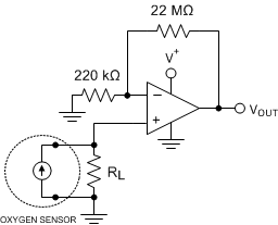
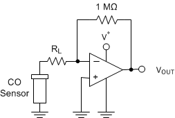
The TLV8811 (single) and TLV8812 (dual) family of precision ultra-low-power operational amplifiers are ideal for cost-optimized, “Always ON” sensing applications in battery powered wireless and low power wired equipment. With 6 kHz of bandwidth from 425 nA of quiescent current and a trimmed offset voltage to under 500µV, the TLV881x amplifiers provide high precision while minimizing power consumption in equipment such as CO gas detectors and portable electronic devices where operational battery-life is critical. They also have a CMOS input stage enabling fempto-amp bias currents, thereby reducing IBIAS and IOS errors that would otherwise impact high source impedance sensing applications. Additionally, built-in EMI protection reduces sensitivity to unwanted RF signals from mobile phones, WiFi, radio transmitters, and tag readers.
The TLV8811 (single) and TLV8812 (dual) channel versions are available in industry standard 5-pin SOT-23 and 8-pin VSSOP packages respectively.
PART NUMBER | PACKAGE | BODY SIZE |
---|---|---|
TLV8811 | SOT-23 (5) | 2.90 mm x 1.60 mm |
TLV8812 | VSSOP (8) | 3.00 mm × 3.00 mm |
PART NUMBER | CHANNELS | SUPPLY CURRENT (Typ per Channel) |
OFFSET VOLTAGE (Max at 25°C) |
---|---|---|---|
LPV811 | 1 | 450 nA | 370 µV |
LPV812 | 2 | 425 nA | 300 µV |
TLV8811 | 1 | 450 nA | 550 µV |
TLV8812 | 2 | 425 nA | 500 µV |
PIN | TYPE | DESCRIPTION | ||
---|---|---|---|---|
NAME | NUMBER | |||
OUT | 1 | O | Output | |
-IN | 4 | I | Inverting Input | |
+IN | 3 | I | Non-Inverting Input | |
V- | 2 | P | Negative (lowest) power supply | |
V+ | 5 | P | Positive (highest) power supply |
PIN | TYPE | DESCRIPTION | ||
---|---|---|---|---|
NAME | NUMBER | |||
OUT A | 1 | O | Channel A Output | |
-IN A | 2 | I | Channel A Inverting Input | |
+IN A | 3 | I | Channel A Non-Inverting Input | |
V- | 4 | P | Negative (lowest) power supply | |
+IN B | 5 | I | Channel B Non-Inverting Input | |
-IN B | 6 | I | Channel B Inverting Input | |
OUT B | 7 | O | Channel B Output | |
V+ | 8 | P | Positive (highest) power supply |
MIN | MAX | UNIT | |||
---|---|---|---|---|---|
Supply voltage, Vs = (V+) - (V-) | –0.3 | 6 | V | ||
Input pins | Voltage (2) (3) | Common mode | (V-) - 0.3 | (V+) + 0.3 | V |
Differential | (V-) - 0.3 | (V+) + 0.3 | V | ||
Input pins | Current | -10 | 10 | mA | |
Output short current (4) | Continuous | Continuous | |||
Storage temperature, Tstg | –65 | 150 | °C | ||
Junction temperature | 150 | °C |
VALUE | UNIT | |||
---|---|---|---|---|
V(ESD) | Electrostatic discharge | Human-body model (HBM), per ANSI/ESDA/JEDEC JS-001(1) | ±1000 | V |
Charged-device model (CDM), per JEDEC specification JESD22-C101(2) | ±250 |
MIN | MAX | UNIT | ||
---|---|---|---|---|
Supply voltage (V+ – V–) | 1.7 | 5.5 | V | |
Specified temperature | -40 | 125 | °C |
THERMAL METRIC(1) | TLV8811 DBV (SOT-23) 5 PINS |
TLV8812 DGK (VSSOP) 8 PINS |
UNIT | |
---|---|---|---|---|
θJA | Junction-to-ambient thermal resistance | 177.4 | 177.6 | ºC/W |
θJCtop | Junction-to-case (top) thermal resistance | 133.9 | 68.8 | |
θJB | Junction-to-board thermal resistance | 36.3 | 98.2 | |
ψJT | Junction-to-top characterization parameter | 23.6 | 12.3 | |
ψJB | Junction-to-board characterization parameter | 35.7 | 96.7 |
VCM = V- | TLV8811 | RL=No Load |
VS= 1.8V | RL= 10MΩ |
VS= 5V | RL= 10MΩ |
VS= 1.8V | TA = -40°C |
VS= 1.8V | TA = 25°C |
VS= 1.8V | TA = 125°C |
VS= 1.8V | RL= No Load |
VS= 3.3V | RL= No Load |
VS= 5V | RL= No Load |
TA = 25 | RL= 10MΩ | Vout = 200mVpp |
VS= ±0.9V | CL= 20pF | AV = +1 |
TA = 25 | RL= 10MΩ | Vout = 1Vpp |
VS= ±0.9V | CL= 20pF | AV = +1 |
TA = 25 | RL= 10MΩ | ΔVCM = 0.5Vpp |
VS= 5V | CL= 20p | |
VCM = Vs/2 | AV = +1 |
TA = -40, 25, 125°C | RL= 10MΩ | VOUT = 200mVPP |
VS= 5V | CL= 20pF | VCM = Vs/2 |
TA = -40, 25, 125°C | RL= 1MΩ | VOUT = 200mVPP |
VS= 5V | CL= 20pF | VCM = Vs/2 |
TA = -40, 25, 125°C | RL= 100kΩ | VOUT = 200mVPP |
VS= 5V | CL= 20pF | VCM = Vs/2 |
TA = -40, 25, 125°C | RL= 10MΩ | VOUT = 200mVPP |
VS= 1.8V | CL= 20pF | VCM = Vs/2 |
TA = -40, 25, 125°C | RL= 1MΩ | VOUT = 200mVPP |
VS= 1.8V | CL= 20pF | VCM = Vs/2 |
TA = -40, 25, 125°C | RL= 100kΩ | VOUT = 200mVPP |
VS= 1.8V | CL= 20pF | VCM = Vs/2 |
VCM = V- | TLV8812 | RL=No Load |
VS= 3.3V | RL= 10MΩ |
VS= 5V | TA = -40 to 125 | VCM = Vs/2 |
VS= 5V | TA = -40°C |
VS= 5V | TA = 25°C |
VS= 5V | TA = 125°C |
VS= 1.8V | RL= No Load |
VS= 3.3V | RL= No Load |
VS= 5V | RL= No Load |
TA = 25 | RL= 10MΩ | Vout = 200mVpp |
VS= ±2.5V | CL= 20pF | AV = +1 |
TA = 25 | RL= 10MΩ | Vout = 2Vpp |
VS= ±2.5V | CL= 20pF | AV = +1 |
TA = 25 | RL= 10MΩ | ΔVS = 0.5Vpp |
VS= 3.3V | CL= 20p | |
VCM = Vs/2 | AV = +1 |
TA = -40, 25, 125°C | RL= 10MΩ | VOUT = 200mVPP |
VS= 3.3V | CL= 20pF | VCM = Vs/2 |
TA = -40, 25, 125°C | RL= 1MΩ | VOUT = 200mVPP |
VS= 3.3V | CL= 20pF | VCM = Vs/2 |
TA = -40, 25, 125°C | RL= 100kΩ | VOUT = 200mVPP |
VS= 3.3V | CL= 20pF | VCM = Vs/2 |
TA = 25°C | VS= 5 V | RL= 10MΩ |
TA = 25 | RL= 1MΩ | VCM = Vs/2 |
VS= 5V | CL= 20pF | AV = +1 |
TA = 25 | RL= 1MΩ | VCM = Vs/2 |
VS= 3.3V | CL= 20pF | AV = +1 |
The TLV8811 (single) and TLV8812 (dual) series of nanoPower CMOS operational amplifiers are designed for long-life battery-powered and energy harvested applications. They operate on a single supply with operation as low as 1.7V. The Input Offset is trimmed to less than 500uV and the output is rail-to-rail and swings to within 3.5mV of the supplies with a 100kΩ load. The common-mode range extends to the negative supply making it ideal for single-supply applications. EMI protection has been employed internally to reduce the effects of EMI.
Parameters that vary significantly with operating voltages or temperature are shown in the Typical Characteristics curves.
The amplifier's differential inputs consist of a non-inverting input (+IN) and an inverting input (–IN). The amplifier amplifies only the difference in voltage between the two inputs, which is called the differential input voltage. The output voltage of the op-amp VOUT is given by Equation 1:
where
The input common-mode voltage range of the TLV881x extends from (V-) to (V+) – 0.9 V. In this range, low offset can be expected with a minimum of 80dB CMRR. The TLV881x is protected from output "inversions" or "reversals".
The TLV881x output voltage swings 3.5 mV from rails at 1.8 V supply, which provides the maximum possible dynamic range at the output. This is particularly important when operating on low supply voltages.
The TLV881x Maximum Output Voltage Swing graph defines the maximum swing possible under a particular output load.
When designing for ultralow power, choose system feedback components carefully. To minimize quiescent current consumption, select large-value feedback resistors. Any large resistors will react with stray capacitance in the circuit and the input capacitance of the operational amplifier. These parasitic RC combinations can affect the stability of the overall system. A feedback capacitor may be required to assure stability and limit overshoot or gain peaking.
When possible, use AC coupling and AC feedback to reduce static current draw through the feedback elements. Use film or ceramic capacitors since large electrolytics may have large static leakage currents in the nanoamps.
The TLV881x is internally compensated for stable unity gain operation, with a 6 kHz typical gain bandwidth. However, the unity gain follower is the most sensitive configuration to capacitive load. The combination of a capacitive load placed directly on the output of an amplifier along with the amplifier’s output impedance creates a phase lag, which reduces the phase margin of the amplifier. If the phase margin is significantly reduced, the response will be under damped which causes peaking in the transfer and, when there is too much peaking, the op amp might start oscillating.
In order to drive heavy (>50pF) capacitive loads, an isolation resistor, RISO, should be used, as shown in Figure 37. By using this isolation resistor, the capacitive load is isolated from the amplifier’s output. The larger the value of RISO, the more stable the amplifier will be. If the value of RISO is sufficiently large, the feedback loop will be stable, independent of the value of CL. However, larger values of RISO result in reduced output swing and reduced output current drive. The recommended value for RISO is 30-50kΩ.
NOTE
Information in the following applications sections is not part of the TI component specification, and TI does not warrant its accuracy or completeness. TI’s customers are responsible for determining suitability of components for their purposes. Customers should validate and test their design implementation to confirm system functionality.
The TLV881x is a ultra-low power operational amplifier that provides 6 kHz bandwidth with only 450nA typical quiescent current, trimmed input offset voltage and precision drift specifications. These rail-to-rail output amplifiers are specifically designed for battery-powered applications. The input common-mode voltage range extends to the negative supply rail and the output swings to within millivolts of the rails, maintaining a wide dynamic range.
Figure 38 shows a simple micropower potentiostat circuit for use with three terminal unbiased CO sensors, though it is applicable to many other type of three terminal gas sensors or electrochemical cells.
The basic sensor has three electrodes; The Sense or Working Electrode (“WE”), Counter Electrode (“CE”) and Reference Electrode (“RE”). A current flows between the CE and WE proportional to the detected concentration.
The RE monitors the potential of the internal reference point. For an unbiased sensor, the WE and RE electrodes must be maintained at the same potential by adjusting the bias on CE. Through the Potentiostat circuit formed by U1, the servo feedback action will maintain the RE pin at a potential set by VREF.
R1 is to maintain stability due to the large capacitance of the sensor. C1 and R2 form the Potentiostat integrator and set the feedback time constant.
U2 forms a transimpedance amplifier ("TIA") to convert the resulting sensor current into a proportional voltage. The transimpedance gain, and resulting sensitivity, is set by RF according to Equation 2.
RL is a load resistor of which the value is normally specified by the sensor manufacturer (typically 10 ohms). The potential at WE is set by the applied VREF. Riso provides capacitive isolation and, combined with C2, form the output filter and ADC reservoir capacitor to drive the ADC.
For this example, we will be using a CO sensor with a sensitivity of 69nA/ppm. The supply voltage and maximum ADC input voltage is 2.5V, and the maximum concentration is 300ppm.
First the VREF voltage must be determined. This voltage is a compromise between maximum headroom and resolution, as well as allowance for "footroom" for the minimum swing on the CE terminal, since the CE terminal generally goes negative in relation to the RE potential as the concentration (sensor current) increases. Bench measurements found the difference between CE and RE to be 180mV at 300ppm for this particular sensor.
To allow for negative CE swing "footroom" and voltage drop across the 10k resistor, 300mV was chosen for VREF.
Therefore +300mV will be used as the minimum VZERO to add some headroom.
where
Next we calculate the maximum sensor current at highest expected concentration:
where
Now find the available output swing range above the reference voltage available for the measurement:
where
Now we calculate the transimpedance resistor ®F) value using the maximum swing and the maximum sensor current:
Figure 39 shows the resulting circuit voltages when the sensor was exposed to 200ppm step of carbon monoxide gas. VC is the monitored CE pin voltage and clearly shows the expected CE voltage dropping below the WE voltage, VW, as the concentration increases.
VTIA is the output of the transimpedance amplifier U2. VDIFF is the calculated difference between VREF and VTIA, which will be used for the ppm calculation.
Figure 40 shows the calculated sensor current using the formula in Equation 7 :
Equation 8 shows the resulting conversion of the sensor current into ppm.
Total supply current for the amplifier section is less than 700 nA, minus sensor current. Note that the sensor current is sourced from the amplifier output, which in turn comes from the amplifier supply voltage. Therefore, any continuous sensor current must also be included in supply current budget calculations.
Do properly bypass the power supplies.
Do add series resistance to the output when driving capacitive loads, particularly cables, Muxes and ADC inputs.
Do add series current limiting resistors and external schottky clamp diodes if input voltage is expected to exceed the supplies. Limit the current to 1mA or less (1KΩ per volt).