SNOSDA9E June 2020 – May 2024 TLV9020-Q1 , TLV9021-Q1 , TLV9022-Q1 , TLV9024-Q1 , TLV9030-Q1 , TLV9031-Q1 , TLV9032-Q1 , TLV9034-Q1
PRODMIX
- 1
- 1 Features
- 2 Applications
- 3 Description
- 4 Pin Configuration and Functions
-
5 Specifications
- 5.1 Absolute Maximum Ratings
- 5.2 ESD Ratings
- 5.3 Recommended Operating Conditions
- 5.4 Thermal Information, TLV90x0-Q1,TLV90x1-Q1
- 5.5 Thermal Information, TLV90x2-Q1
- 5.6 Thermal Information, TLV90x4-Q1
- 5.7 Electrical Characteristics, TLV90x0-Q1,TLV90x1-Q1
- 5.8 Switching Characteristics, TLV90x0-Q1,TLV90x1-Q1
- 5.9 Electrical Characteristics, TLV90x2-Q1
- 5.10 Switching Characteristics, TLV90x2-Q1
- 5.11 Electrical Characteristics, TLV90x4-Q1
- 5.12 Switching Characteristics, TLV90x4-Q1
- 5.13 Typical Characteristics
- 6 Detailed Description
-
7 Application and Implementation
- 7.1 Application Information
- 7.2 Typical Applications
- 7.3 Power Supply Recommendations
- 8 Layout
- 9 Device and Documentation Support
- 10Revision History
- 11Mechanical, Packaging, and Orderable Information
Package Options
Mechanical Data (Package|Pins)
Thermal pad, mechanical data (Package|Pins)
Orderable Information
7.2.9 Pulse Slicer
A Pulse Slicer is a variation of the Zero Crossing Detector and is used to detect the zero crossings on an input signal with a varying baseline level. This circuit works best with symmetrical waveforms. The RC network of R1 and C1 establishes an mean reference voltage VREF, which tracks the mean amplitude of the VIN signal. The noninverting input is directly connected to VREF through R2. R2 and R3 are used to produce hysteresis to keep transitions free of spurious toggles. The time constant is a tradeoff between long-term symmetry and response time to changes in amplitude.
When the waveform is data, TI recommends that the data be encoded in NRZ (Non-Return to Zero) format to maintain proper average baseline. Asymmetrical inputs may suffer from timing distortions caused by the changing VREF average voltage.
 Figure 7-18 Pulse Slicer Using
TLV903x-Q1
Figure 7-18 Pulse Slicer Using
TLV903x-Q1For this design, follow these design requirements:
- The RC constant value (R2 and C1) must support the targeted data rate to maintain a valid tripping threshold.
- The hysteresis introduced with R2 and R43 helps to avoid spurious output toggles.
The TLV902x-Q1 can also be used, but with the addition of a pull-up resistor on the output (not shown for clarity).
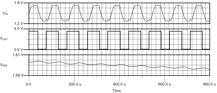
Figure 7-19 shows the results of a 9600 baud data signal riding on a varying baseline.
 Figure 7-19 Pulse Slicer Waveforms