SNOSDA3G June 2020 – February 2025 TLV9020 , TLV9021 , TLV9022 , TLV9024 , TLV9030 , TLV9031 , TLV9032 , TLV9034
PRODMIX
- 1
- 1 Features
- 2 Applications
- 3 Description
- 4 Pin Configuration and Functions
-
5 Specifications
- 5.1 Absolute Maximum Ratings
- 5.2 ESD Ratings
- 5.3 Recommended Operating Conditions
- 5.4 Thermal Information, TLV90x0,TLV90x1
- 5.5 Thermal Information, TLV90x2
- 5.6 Thermal Information, TLV90x4
- 5.7 Electrical Characteristics, TLV90x0,TLV90x1
- 5.8 Switching Characteristics, TLV90x0,TLV90x1
- 5.9 Electrical Characteristics, TLV90x2
- 5.10 Switching Characteristics, TLV90x2
- 5.11 Electrical Characteristics, TLV90x4
- 5.12 Switching Characteristics, TLV90x4
- 5.13 Typical Characteristics
- 6 Detailed Description
-
7 Application and Implementation
- 7.1 Application Information
- 7.2 Typical Applications
- 7.3 Power Supply Recommendations
- 7.4 Layout
- 8 Device and Documentation Support
- 9 Revision History
- 10Mechanical, Packaging, and Orderable Information
Package Options
Mechanical Data (Package|Pins)
Thermal pad, mechanical data (Package|Pins)
- DSG|8
Orderable Information
3 Description
The TLV902x and TLV903x are a family of single, dual and quad channel comparators. The family offers low input offset voltage, fault-tolerant inputs and a excellent speed-to-power combination. The family has a propagation delay of 100ns with a quiescent supply current of only 18μA per channel.
The family also includes a Power-on Reset (POR) feature that makes sure the output is in a known state until the minimum supply voltage has been reached. This prevents output transients during system power-up and power-down.
These comparators also feature fault-tolerant inputs that can go up to 6V without damage and with no output phase inversion. This family of comparators is designed for precision voltage monitoring in harsh, noisy environments.
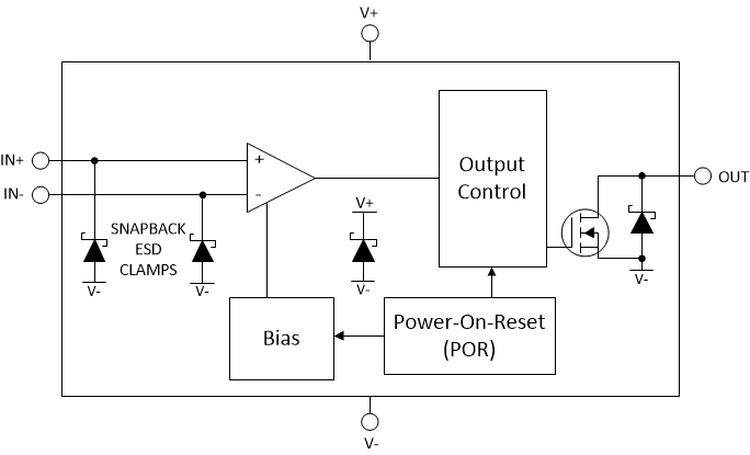
The TLV902x have an open-drain output that can be pulled-up below or beyond the supply voltage. These devices are designed for low voltage logic translators.
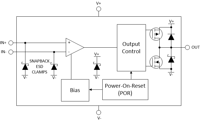
The TLV903x have a push-pull output stage capable of sinking and sourcing many milliamps of current to drive LEDs or capacitive loads for MOSFET gates.
The TLV90x0 and TLV90x1 are alternate pinouts of the single device.
The family is specified for the Industrial temperature range of -40°C to +125°C and are available in a standard leaded and leadless packages.
| PART NUMBER | PACKAGE (1) | BODY SIZE (NOM) (2) |
|---|---|---|
TLV90x0, | SC-70 (5) | 1.25mm x 2.00mm |
| SOT-23 (5) | 1.60mm x 2.90mm | |
| TLV9022, TLV9032 (Dual) | SOIC (8) | 3.91mm × 4.90mm |
| TSSOP (8) | 3.00mm × 4.40mm | |
| VSSOP (8) | 3.00mm × 3.00mm | |
WSON (8) | 2.00mm × 2.00mm | |
| SOT-23 (8) | 1.60mm × 2.90mm | |
| TLV9024, TLV9034 (Quad) | SOIC (14) | 3.91mm × 8.65mm |
| TSSOP (14) | 4.40mm × 5.00mm | |
| SOT-23 (14) | 4.20mm x 2.00mm | |
| WQFN (16) | 3.00mm × 3.00mm | |
X2QFN (14)(Preview) | 2.00mm x 2.00mm |
 TLV902x Block Diagram
 TLV903x Block Diagram