SBOS836G March 2020 – March 2022 TLV9041 , TLV9042 , TLV9044
PRODUCTION DATA
- 1 Features
- 2 Applications
- 3 Description
- 4 Revision History
- 5 Device Comparison Table
- 6 Pin Configuration and Functions
- 7 Specifications
-
8 Detailed Description
- 8.1 Overview
- 8.2 Functional Block Diagram
- 8.3
Feature Description
- 8.3.1 Operating Voltage
- 8.3.2 Rail-to-Rail Input
- 8.3.3 Rail-to-Rail Output
- 8.3.4 Common-Mode Rejection Ratio (CMRR)
- 8.3.5 Capacitive Load and Stability
- 8.3.6 Overload Recovery
- 8.3.7 EMI Rejection
- 8.3.8 Electrical Overstress
- 8.3.9 Input and ESD Protection
- 8.3.10 Shutdown Function
- 8.3.11 Packages With an Exposed Thermal Pad
- 8.4 Device Functional Modes
- 9 Application and Implementation
- 10Power Supply Recommendations
- 11Layout
- 12Device and Documentation Support
- 13Mechanical, Packaging, and Orderable Information
Package Options
Mechanical Data (Package|Pins)
Thermal pad, mechanical data (Package|Pins)
- DPW|5
Orderable Information
8.3.8 Electrical Overstress
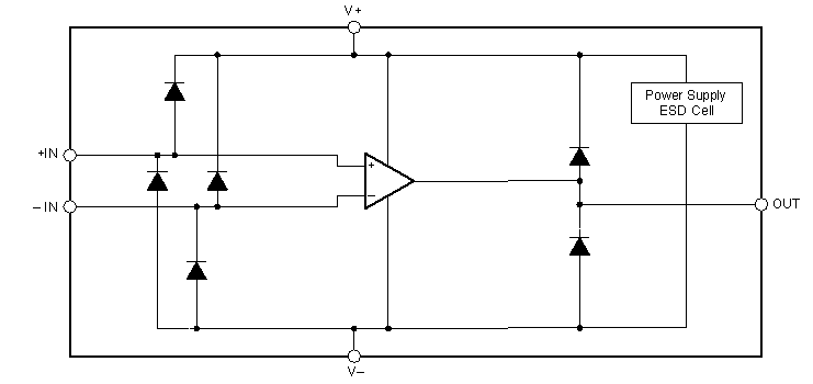
Designers often ask questions about the capability of an operational amplifier to withstand electrical overstress. These questions tend to focus on the device inputs, but can involve the supply voltage pins or even the output pin. Each of these different pin functions have electrical stress limits determined by the voltage breakdown characteristics of the particular semiconductor fabrication process and specific circuits connected to the pin. Additionally, internal electrostatic discharge (ESD) protection is built into these circuits to protect them from accidental ESD events both before and during product assembly.
Having a good understanding of this basic ESD circuitry and its relevance to an electrical overstress event is helpful. Figure 8-5 shows the ESD circuits contained in the TLV904x devices. The ESD protection circuitry involves several current-steering diodes connected from the input and output pins and routed back to the internal power supply lines, where they meet at an absorption device internal to the operational amplifier. This protection circuitry is intended to remain inactive during normal circuit operation.
 Figure 8-5 Equivalent Internal ESD
Circuitry