SBOS942J August 2018 – February 2024 TLV9051 , TLV9052 , TLV9054
PRODUCTION DATA
- 1
- 1 Features
- 2 Applications
- 3 Description
- 4 Device Comparison Table
- 5 Pin Configuration and Functions
-
6 Specifications
- 6.1 Absolute Maximum Ratings
- 6.2 ESD Ratings
- 6.3 Recommended Operating Conditions
- 6.4 Thermal Information for Single Channel
- 6.5 Thermal Information for Dual Channel
- 6.6 Thermal Information for Quad Channel
- 6.7 Electrical Characteristics: VS (Total Supply Voltage) = (V+) – (V–) = 1.8 V to 5.5 V
- 6.8 Typical Characteristics
- 7 Detailed Description
- 8 Application and Implementation
- 9 Device and Documentation Support
- 10Revision History
- 11Mechanical, Packaging, and Orderable Information
Package Options
Mechanical Data (Package|Pins)
Thermal pad, mechanical data (Package|Pins)
- DPW|5
Orderable Information
3 Description
The TLV9051, TLV9052, and TLV9054 devices are single, dual, and quad operational amplifiers, respectively. The devices are designed for low voltage operation from 1.8V to 6.0V. The inputs and outputs can operate from rail to rail at a very high slew rate. These devices are an excellent choice for cost-constrained applications where low-voltage operation, high slew rate, and low quiescent current is needed. The capacitive-load drive of the TLV905x family is 150pF, and the resistive open-loop output impedance makes stabilization easier with much higher capacitive loads.
The TLV905xS devices include a shutdown mode that allow the amplifiers to be switched off into a standby mode with typical current consumption less than 1µA.
The TLV905x family is easy to use due to the devices being unity-gain stable, including a RFI and EMI filter, and being free from phase reversal in an overdrive condition.
| PART NUMBER(1) | CHANNEL COUNT | PACKAGE(2) | PACKAGE SIZE(4) |
|---|---|---|---|
| TLV9051 | Single | DBV (SOT-23, 5) | 2.9mm × 2.8mm |
| DCK (SC70, 5) | 2mm × 2.1mm | ||
| DRL (SOT553, 5)(3) | 1.6mm × 1.6mm | ||
| DPW (X2SON, 5) | 0.8mm × 0.8mm | ||
| TLV9051S | Single, Shutdown | DBV (SOT-23, 6) | 2.9mm × 2.8mm |
| TLV9052 | Dual | D (SOIC, 8) | 4.9mm × 6mm |
| PW (TSSOP, 8) | 3.mm × 6.4mm | ||
| DGK (VSSOP, 8) | 3mm × 4.9mm | ||
| DDF (SOT-23, 8) | 2.9mm × 2.8mm | ||
| DSG (WSON, 8) | 2mm × 2mm | ||
| TLV9052S | Dual, Shutdown | DGS (VSSOP, 10) | 3mm × 4.9mm |
| RUG (X2QFN, 10) | 1.5mm × 2mm | ||
| TLV9054 | Quad | D (SOIC, 14) | 8.65mm × 6mm |
| PW (TSSOP, 14) | 5mm × 6.4mm | ||
| RUC (WQFN, 14) | 2mm × 2mm | ||
| RTE (WQFN, 16) | 3mm × 3mm | ||
| TLV9054S | Quad, Shutdown | RTE (WQFN, 16) | 3mm × 3mm |
 Single-Pole, Low-Pass
Filter
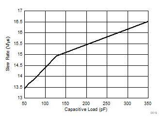
 Slew Rate vs Load
Capacitance