SBOSAH8B February 2024 – May 2024 TLV9051-Q1 , TLV9052-Q1
PRODMIX
- 1
- 1 Features
- 2 Applications
- 3 Description
- 4 Pin Configuration and Functions
-
5 Specifications
- 5.1 Absolute Maximum Ratings
- 5.2 ESD Ratings
- 5.3 Recommended Operating Conditions
- 5.4 Thermal Information for Single Channel
- 5.5 Thermal Information for Dual Channel
- 5.6 Thermal Information for Quad Channel
- 5.7 Electrical Characteristics: VS (Total Supply Voltage) = (V+) – (V–) = 1.8V to 5.5V
- 5.8 Typical Characteristics
- 6 Detailed Description
- 7 Application and Implementation
- 8 Device and Documentation Support
- 9 Revision History
- 10Mechanical, Packaging, and Orderable Information
Package Options
Refer to the PDF data sheet for device specific package drawings
Mechanical Data (Package|Pins)
- PW|8
Thermal pad, mechanical data (Package|Pins)
Orderable Information
5.8 Typical Characteristics
at TA = 25°C, VS = 5.5V, RL = 10kΩ connected to VS / 2, VCM = VS / 2, and VOUT = VS / 2 (unless otherwise noted)
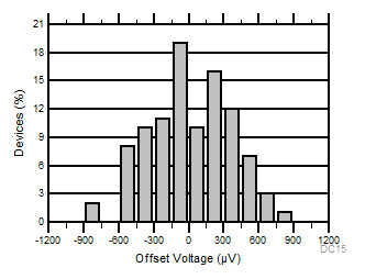
| VS = 5.5V |
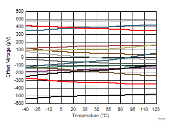 Figure 5-3 Offset Voltage vs Temperature
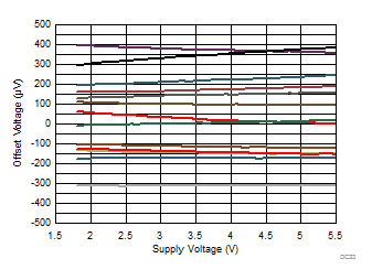 Figure 5-5 Offset Voltage vs Power Supply
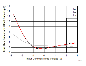 Figure 5-7 Input
Bias Current and Offset Current vs Common-Mode Voltage
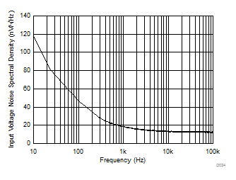 Figure 5-9 Input
Voltage Noise Spectral Density vs Frequency
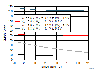
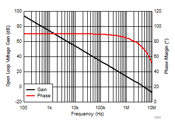 Figure 5-13 Open
Loop Voltage Gain and Phase vs Frequency
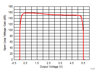 Figure 5-15 Open
Loop Voltage Gain vs Output Voltage
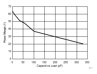 Figure 5-17 Phase
Margin vs Capacitive Load
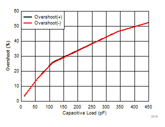
| G = +1V/V | ||
| VOUT step = 100mVp-p | ||
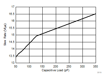
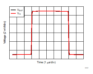
| G = +1V/V | ||
| VOUT step = 10mVp-p |
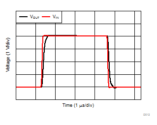
| G = +1V/V | ||
| VOUT step = 4Vp-p |
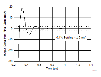
| CL = 100pF | G = +1V/V | |
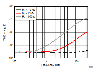
| VOUT = 0.5VRMS | G = +1 | VCM = 2.5V |
| BW = 80kHz |
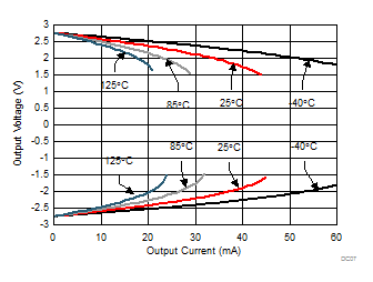 Figure 5-31 Output Voltage Swing vs Output Current
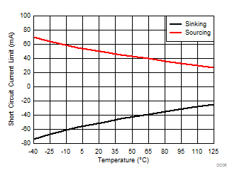 Figure 5-33 Short-Circuit Current vs Temperature
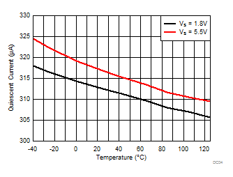 Figure 5-35 Quiescent Current vs Temperature
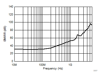
| PRF = –10dBm | ||
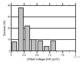
| VS = 5.5V, TA = –40°C to 125°C |
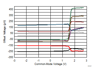 Figure 5-4 Offset Voltage vs Common-Mode Voltage
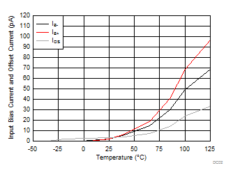 Figure 5-6 Input
Bias Current vs Temperature
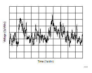 Figure 5-8 0.1Hz
to 10Hz Input Voltage Noise
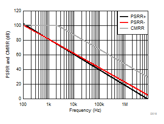 Figure 5-10 CMRR
and PSRR vs Frequency (Referred to Input)
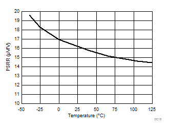
| VS = 1.8V to 5.5V |
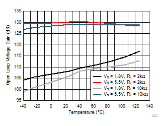 Figure 5-14 Open
Loop Voltage Gain vs Temperature
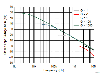 Figure 5-16 Closed Loop Voltage Gain vs Frequency
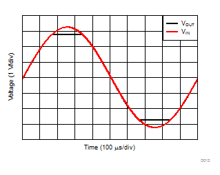 Figure 5-18 No
Phase Reversal
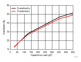
| G = –1V/V | ||
| VOUT step = 100mVp-p |
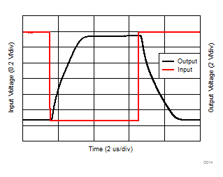
| G = –10V/V |
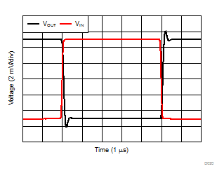
| G = –1V/V | ||
| VOUT step = 10mVp-p |
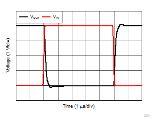
| G = –1V/V | ||
| VOUT step = 4Vp-p |
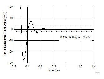
| CL = 100pF | G = +1V/V | |
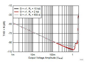
| f = 1kHz | G = +1 | VCM = 2.5V |
| BW = 80kHz |
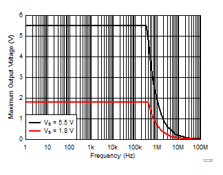 Figure 5-32 Maximum Output Voltage vs Frequency and Supply Voltage
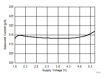 Figure 5-34 Quiescent Current vs Supply Voltage
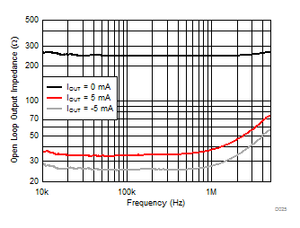 Figure 5-36 Open-Loop Output Impedance vs Frequency
| PRF = –10dBm | ||