SBOSAJ3 June 2024 TLV9104-Q1
PRODMIX
- 1
- 1 Features
- 2 Applications
- 3 Description
- 4 Pin Configuration and Functions
- 5 Specifications
- 6 Detailed Description
- 7 Application and Implementation
- 8 Device and Documentation Support
- 9 Revision History
- 10Mechanical, Packaging, and Orderable Information
Package Options
Mechanical Data (Package|Pins)
- PW|14
Thermal pad, mechanical data (Package|Pins)
Orderable Information
3 Description
The TLV910x-Q1 family (TLV9101-Q1, TLV9102-Q1, and TLV9104-Q1) is a family of 16V general purpose operational amplifiers. This family offers excellent DC precision and AC performance, including rail-to-rail input/output, low offset (±300µV, typical), low offset drift (±0.6µV/°C, typical), and 1.1MHz bandwidth.
Wide differential and common-mode input-voltage range, high output current (±80mA, typical), high slew rate (4.5V/µs, typical), and low power operation (115µA, typical)make the TLV910x-Q1 a robust, low-power, high-performance operational amplifier for automotive applications.
The TLV910x-Q1 family of op amps is available in several packages, and is specified from –40°C to 125°C.
| PART NUMBER (1) | CHANNEL COUNT | PACKAGE | PACKAGE SIZE (4) |
|---|---|---|---|
| TLV9101-Q1(2) | Single | DBV (SOT-23, 5(3) | 2.9mm × 2.8mm |
| DCK (SC70, 5)(3) | 2mm × 2.1mm | ||
| TLV9102-Q1(2) | Dual | D (SOIC, 8)(3) | 4.9mm × 6mm |
| DGK (VSSOP, 8)(3) | 3mm × 4.9mm | ||
| TLV9104-Q1 | Quad | D (SOIC, 14)(3) | 8.65mm × 6mm |
| PW (TSSOP, 14) | 5mm × 6.4mm |
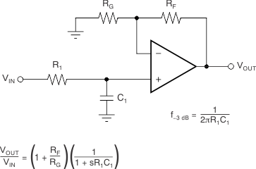
 TLV910x-Q1 in a Single-Pole, Low-Pass Filter