at TA = 25°C, VS = ±8V,
VCM = VS / 2, RLOAD = 10kΩ (unless otherwise noted)
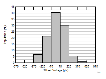
| Distribution from 74 amplifiers, TA = 25°C |
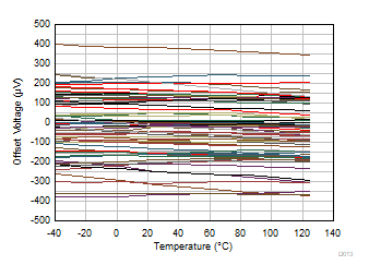
| VCM = V– |
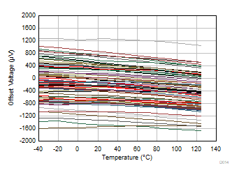
| Data from 74 amplifiers |
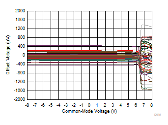
| TA = 25°C |
| Data from 74 amplifiers |

| TA = 125°C |
| Data from 74 amplifiers |

| TA = –40°C |
| Data from 74 amplifiers |

| VCM = V– |
| Data from 74 amplifiers |
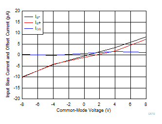 Figure 5-13 Input Bias
Current and Offset Current vs Common-Mode Voltage
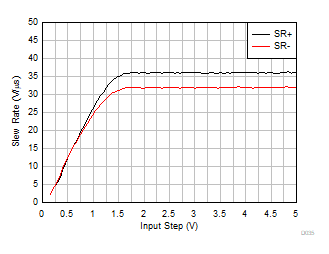 Figure 5-15 Slew Rate vs
Input Step Voltage
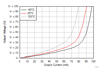 Figure 5-17 Output Voltage
Swing vs Output Current (Sinking)
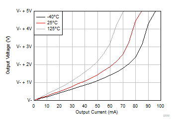 Figure 5-19 Output Voltage
Swing vs Output Current (Sinking)
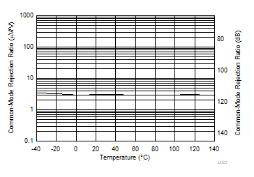 Figure 5-21 CMRR vs
Temperature
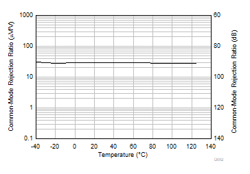 Figure 5-23 CMRR vs Temperature
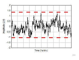 Figure 5-25 0.1Hz to 10Hz
Noise
 Figure 5-27 Quiescent
Current vs Supply Voltage
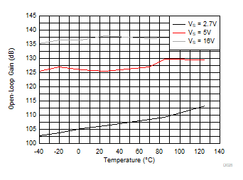 Figure 5-29 Open-Loop
Voltage Gain vs Temperature (dB)
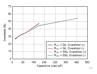
| 20mVpp
output step, G = –1 |
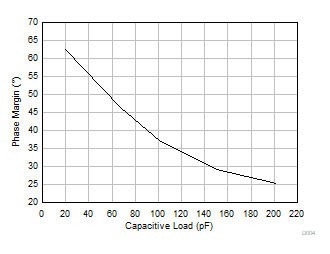 Figure 5-33 Phase Margin vs
Capacitive Load
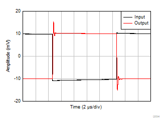
| CL =
20pF, G = –1, 20mVpp step response |
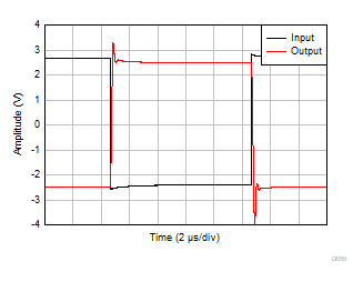
| CL =
20pF, G = –1, 5Vpp step response |
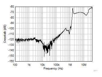 Figure 5-39 Channel
Separation vs Frequency
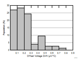
| Distribution from 74 amplifiers |
| VCM = V+ |
| Data from 74 amplifiers |
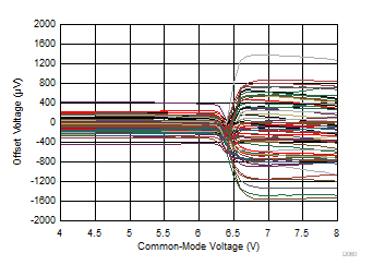
| TA = 25°C |
| Data from 74 amplifiers |

| TA = 125°C |
| Data from 74 amplifiers |

| TA = –40°C |
| Data from 74 amplifiers |
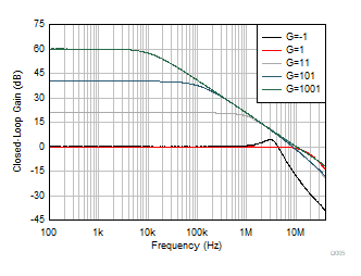 Figure 5-12 Closed-Loop
Gain vs Frequency
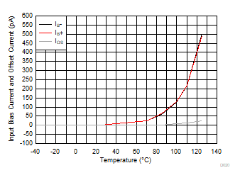 Figure 5-14 Input Bias
Current and Offset Current vs Temperature
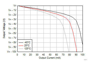 Figure 5-16 Output Voltage
Swing vs Output Current (Sourcing)
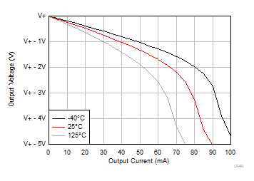 Figure 5-18 Output Voltage
Swing vs Output Current (Sourcing)
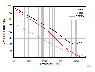 Figure 5-20 CMRR and PSRR
vs Frequency
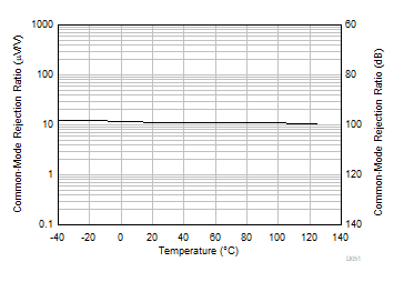 Figure 5-22 CMRR vs
Temperature
 Figure 5-24 PSRR vs
Temperature
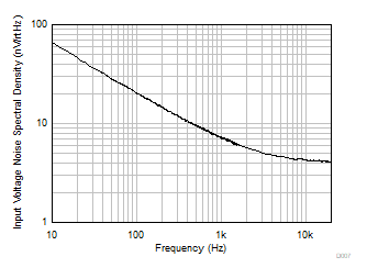 Figure 5-26 Input Voltage
Noise Spectral Density vs Frequency
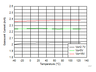 Figure 5-28 Quiescent
Current vs Temperature
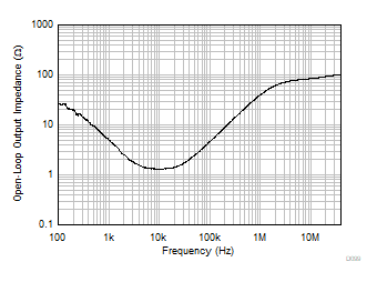 Figure 5-30 Open-Loop
Output Impedance vs Frequency
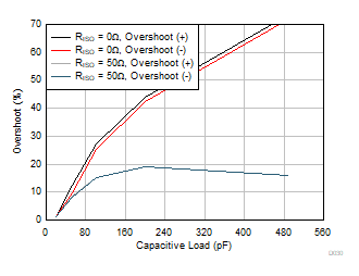
| 20mVpp
output step, G = +1 |
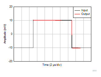
| CL =
20pF, G = 1, 20mVpp step response |
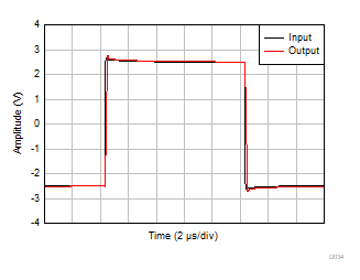
| CL =
20pF, G = 1, 5Vpp step response |
 Figure 5-38 Maximum Output
Voltage vs Frequency
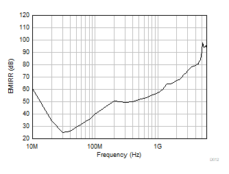 Figure 5-40 EMIRR
(Electromagnetic Interference Rejection Ratio) vs Frequency


 Figure 5-15 Slew Rate vs
Input Step Voltage


 Figure 5-25 0.1Hz to 10Hz
Noise
 Figure 5-29 Open-Loop
Voltage Gain vs Temperature (dB)


 Figure 5-39 Channel
Separation vs Frequency


 Figure 5-20 CMRR and PSRR
vs Frequency
 Figure 5-24 PSRR vs
Temperature
 Figure 5-26 Input Voltage
Noise Spectral Density vs Frequency
 Figure 5-30 Open-Loop
Output Impedance vs Frequency


 Figure 5-38 Maximum Output
Voltage vs Frequency
 Figure 5-40 EMIRR
(Electromagnetic Interference Rejection Ratio) vs Frequency