SBOSA68D November 2021 – March 2024 TLV9161 , TLV9162 , TLV9164
PRODUCTION DATA
- 1
- 1 Features
- 2 Applications
- 3 Description
- 4 Pin Configuration and Functions
- 5 Specifications
-
6 Detailed Description
- 6.1 Overview
- 6.2 Functional Block Diagram
- 6.3
Feature Description
- 6.3.1 Input Protection Circuitry
- 6.3.2 EMI Rejection
- 6.3.3 Thermal Protection
- 6.3.4 Capacitive Load and Stability
- 6.3.5 Common-Mode Voltage Range
- 6.3.6 Phase Reversal Protection
- 6.3.7 Electrical Overstress
- 6.3.8 Overload Recovery
- 6.3.9 Typical Specifications and Distributions
- 6.3.10 Packages With an Exposed Thermal Pad
- 6.3.11 Shutdown
- 6.4 Device Functional Modes
- 7 Application and Implementation
- 8 Device and Documentation Support
- 9 Revision History
- 10Mechanical, Packaging, and Orderable Information
Package Options
Mechanical Data (Package|Pins)
Thermal pad, mechanical data (Package|Pins)
- DSG|8
Orderable Information
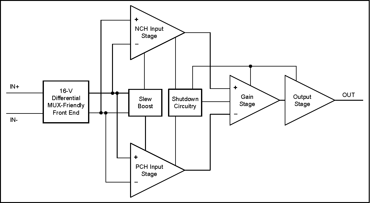
6.2 Functional Block Diagram
