SBOSAJ4 June 2024 TLV9304-Q1
PRODMIX
- 1
- 1 Features
- 2 Applications
- 3 Description
- 4 Pin Configuration and Functions
- 5 Specifications
- 6 Detailed Description
- 7 Application and Implementation
- 8 Device and Documentation Support
- 9 Revision History
- 10Mechanical, Packaging, and Orderable Information
Package Options
Mechanical Data (Package|Pins)
- PW|14
Thermal pad, mechanical data (Package|Pins)
Orderable Information
3 Description
The TLV930x-Q1 family (TLV9301-Q1, TLV9302-Q1, and TLV9304-Q1) is a family of 40V, cost-optimized operational amplifiers. These devices offer strong general-purpose DC and AC specifications, including rail-to-rail output, low offset (±0.5mV, typical), low offset drift (±2µV/°C, typical), and 1MHz bandwidth.
Convenient features such as wide differential input-voltage range, high output current (±60mA), and high slew rate (3V/µs) make the TLV930x-Q1 a robust operational amplifier for high-voltage, cost-sensitive applications.
The TLV930x-Q1 family of op amps is available in standard packages and is specified from –40°C to 125°C.
Device Information
| PART NUMBER(1) | CHANNEL COUNT | PACKAGE | PACKAGE SIZE(2) |
|---|---|---|---|
| TLV9301-Q1(4) | Single | DBV (SOT-23, 5)(3) | 2.9mm × 2.8mm |
| DCK (SC70, 5)(3) | 2mm × 2.1mm | ||
| TLV9302-Q1(4) | Dual | D (SOIC, 8)(3) | 4.9mm × 6mm |
| PW (TSSOP, 8)(3) | 3mm × 6.4mm | ||
| TLV9304-Q1 | Quad | D (SOIC, 14)(3) | 8.65mm × 6mm |
| PW (TSSOP, 14) | 5mm × 6.4mm |
(1) For all available packages, see the orderable addendum at the end of the data sheet.
(2) The package size (length × width) is a nominal value and includes pins, where applicable.
(3) This package is preview only.
(4) This device is preview only.
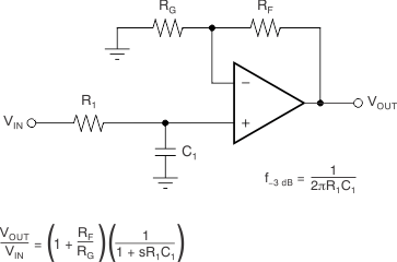
 TLV930x-Q1 in a Single-Pole, Low-Pass Filter