at TA = 25°C,
VS = ±20V, VCM = VS / 2, RLOAD =
10kΩ connected to VS / 2, and CL = 100pF (unless otherwise
noted)
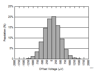 Figure 5-1 Offset Voltage
Production Distribution
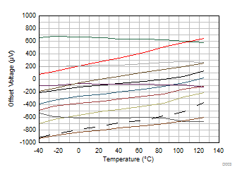 Figure 5-3 Offset Voltage
vs Temperature
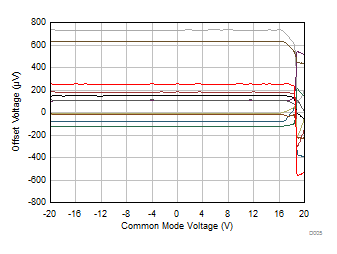 Figure 5-5 Offset Voltage
vs Common-Mode Voltage
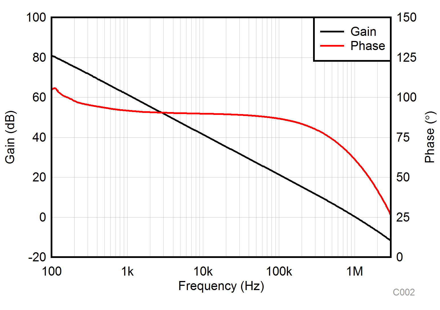 Figure 5-7 Open-Loop Gain
and Phase vs Frequency
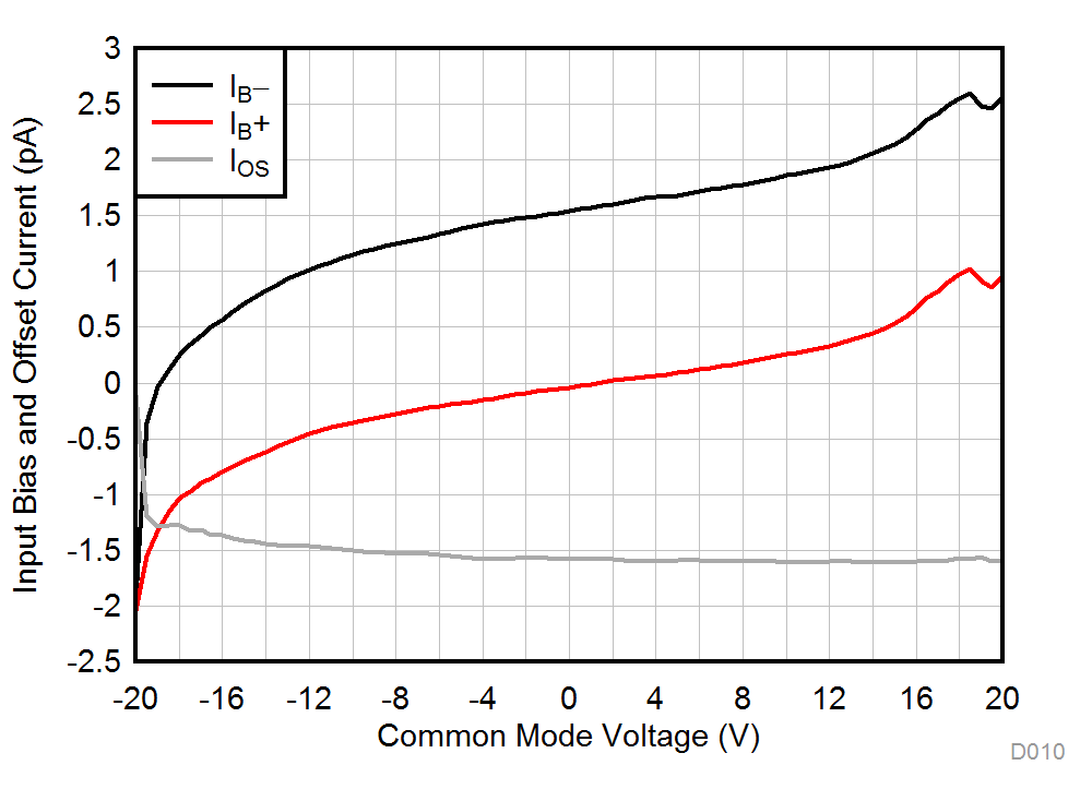 Figure 5-9 Input Bias
Current vs Common-Mode Voltage
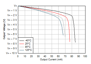 Figure 5-11 Output Voltage
Swing vs Output Current (Sourcing)
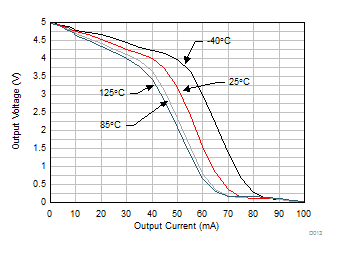 Figure 5-13 Output Voltage
Swing vs Output Current (Sourcing)
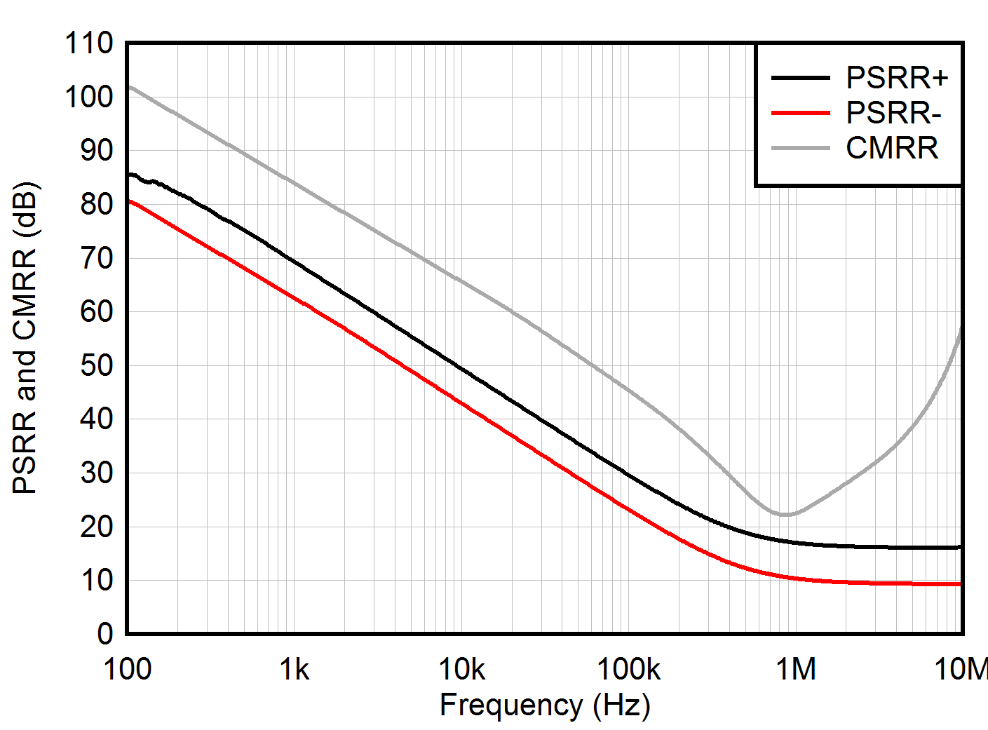 Figure 5-15 CMRR and PSRR
vs Frequency
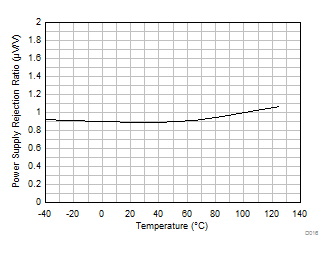 Figure 5-17 PSRR vs
Temperature (dB)
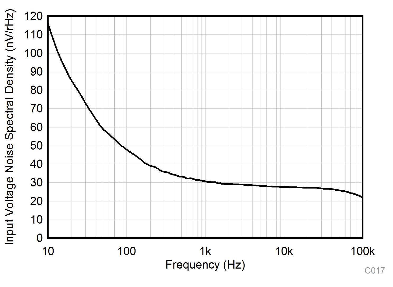 Figure 5-19 Input Voltage
Noise Spectral Density vs Frequency
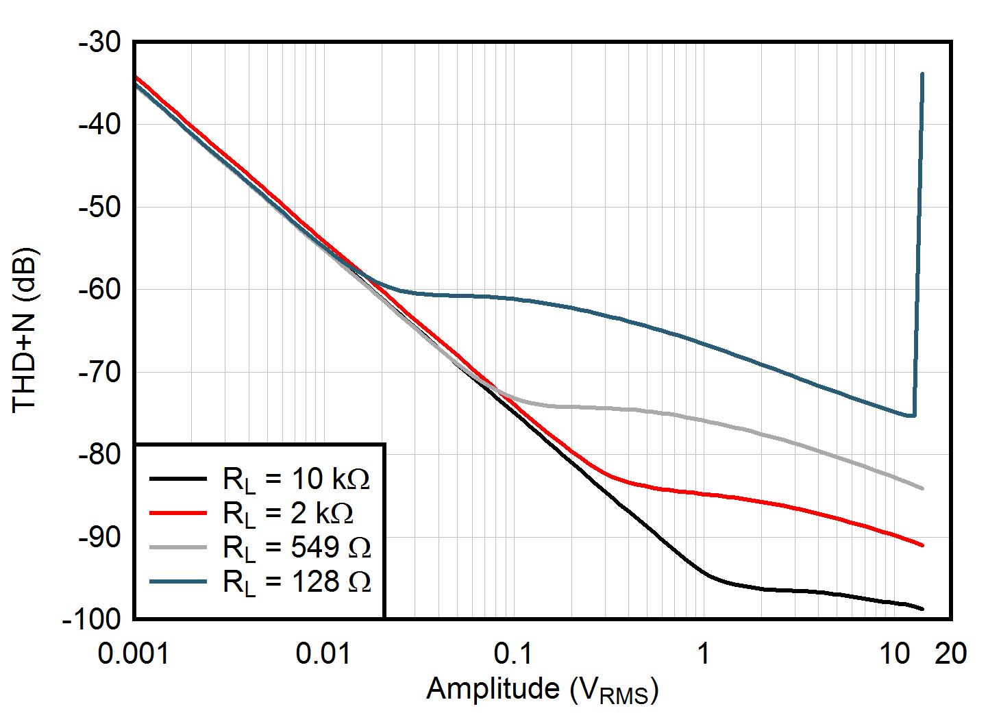 Figure 5-21 THD+N vs Output
Amplitude
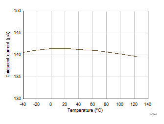 Figure 5-23 Quiescent
Current vs Temperature
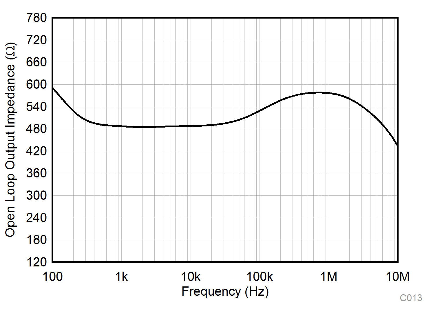 Figure 5-25 Open-Loop
Output Impedance vs Frequency
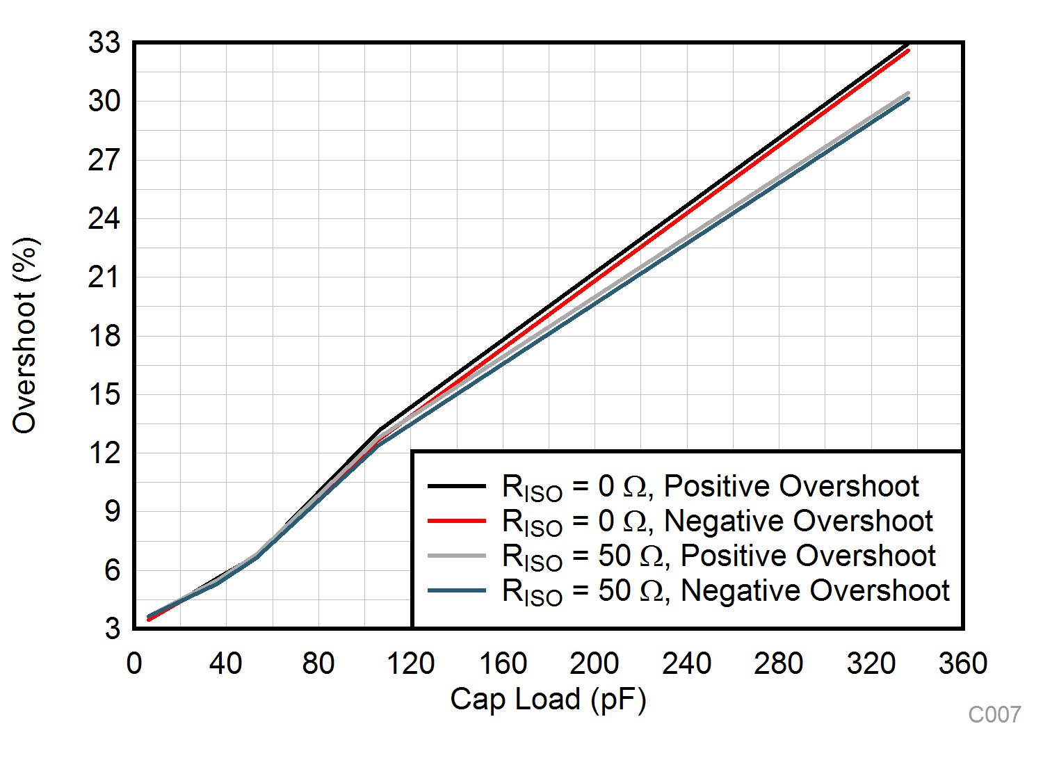
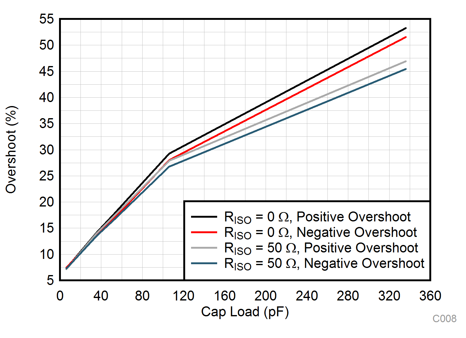 Figure 5-27 Small-Signal
Overshoot vs Capacitive Load
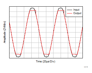 Figure 5-29 No Phase
Reversal
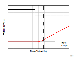 Figure 5-31 Negative
Overload Recovery
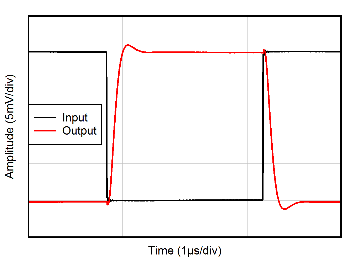
| RL =
1kΩ, CL = 20pF, G = –1, 10mV step
response |
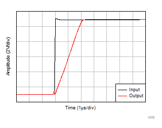 Figure 5-35 Large-Signal
Step Response (Rising)
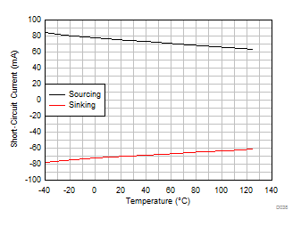 Figure 5-37 Short-Circuit
Current vs Temperature
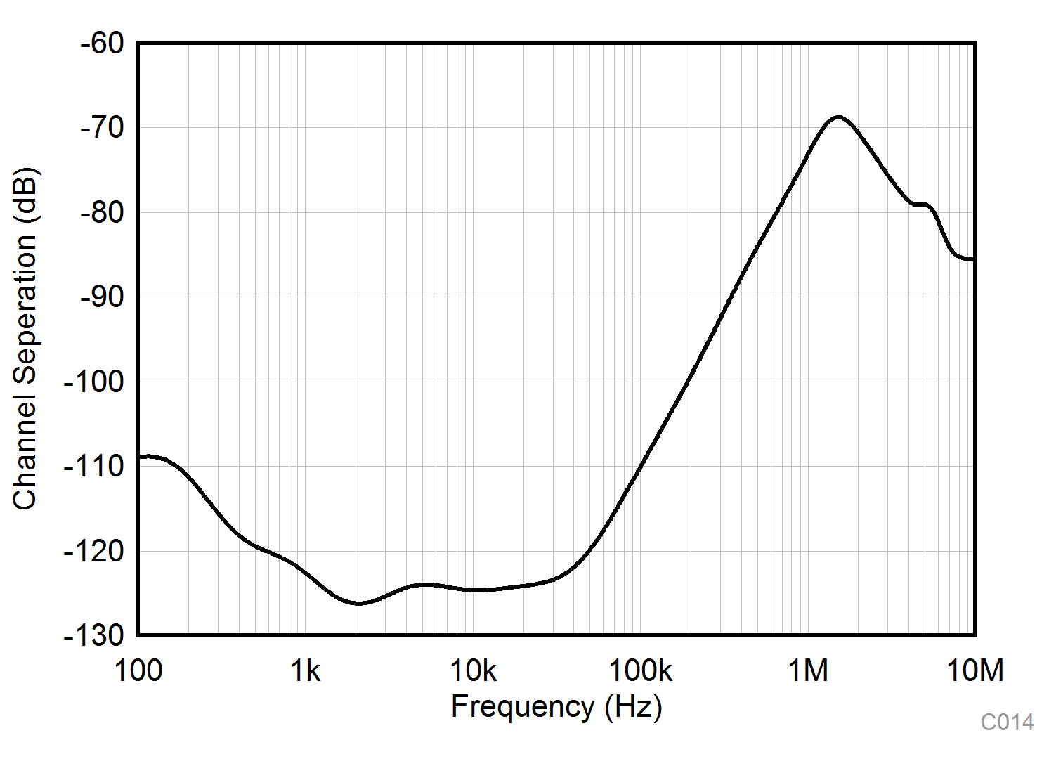 Figure 5-39 Channel
Separation vs Frequency
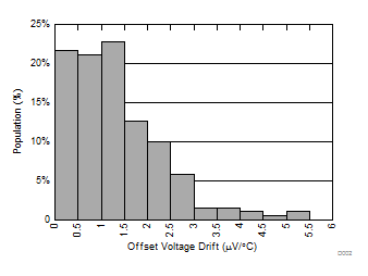 Figure 5-2 Offset Voltage
Drift Distribution
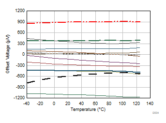 Figure 5-4 Offset Voltage
vs Temperature
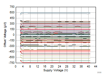 Figure 5-6 Offset Voltage
vs Power Supply
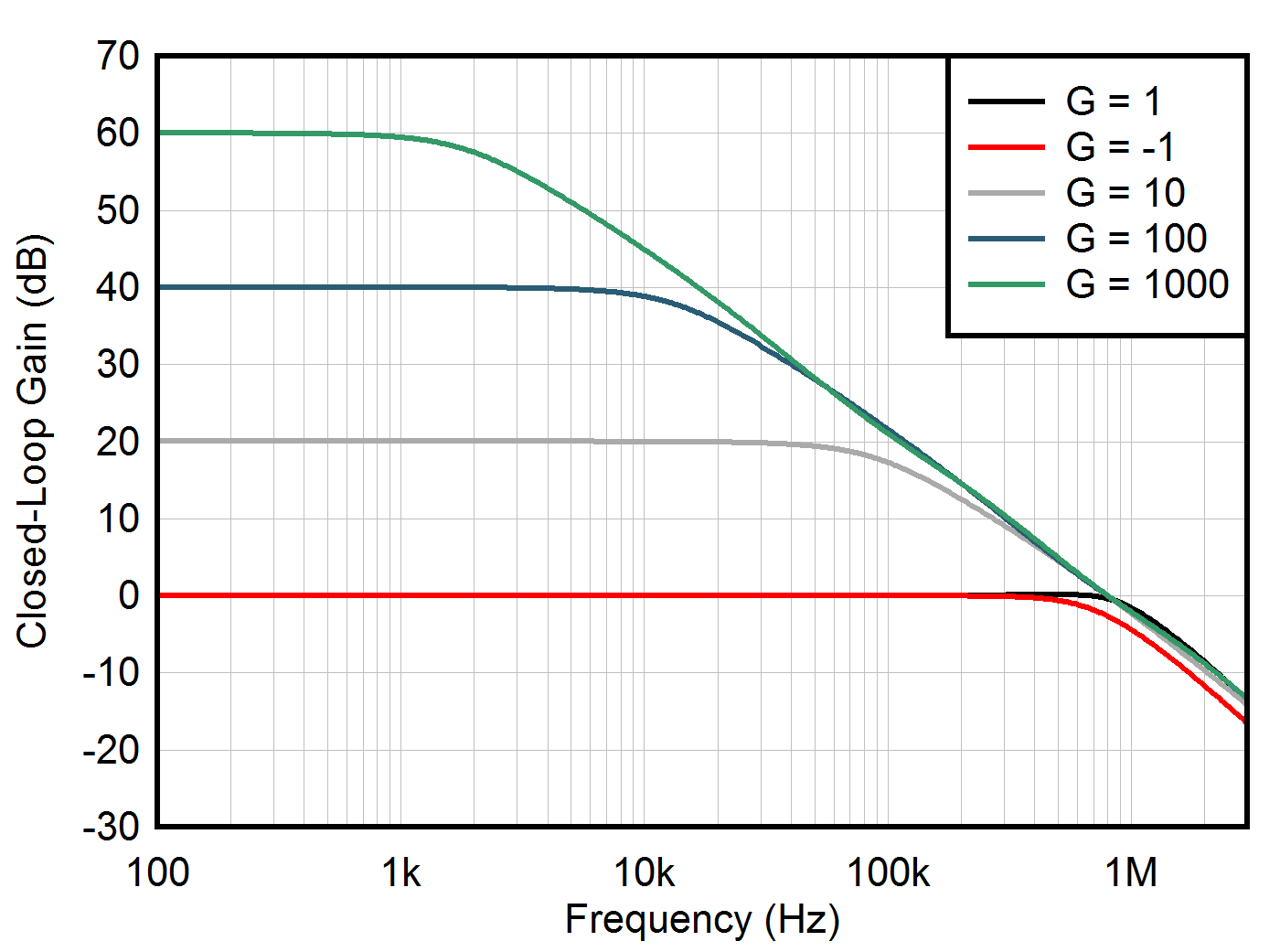 Figure 5-8 Closed-Loop
Gain and Phase vs Frequency
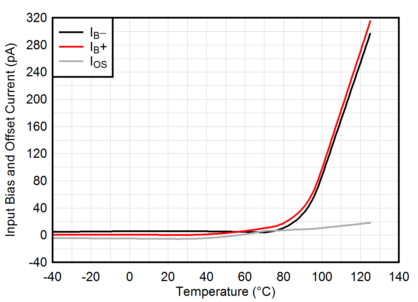 Figure 5-10 Input Bias
Current vs Temperature
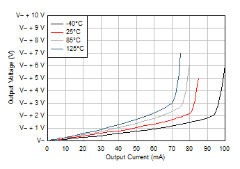 Figure 5-12 Output Voltage
Swing vs Output Current (Sinking)
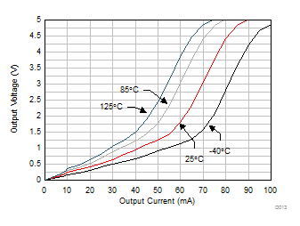 Figure 5-14 Output Voltage
Swing vs Output Current (Sinking)
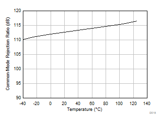 Figure 5-16 CMRR vs
Temperature (dB)
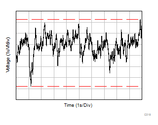 Figure 5-18 0.1Hz to 10Hz
Noise
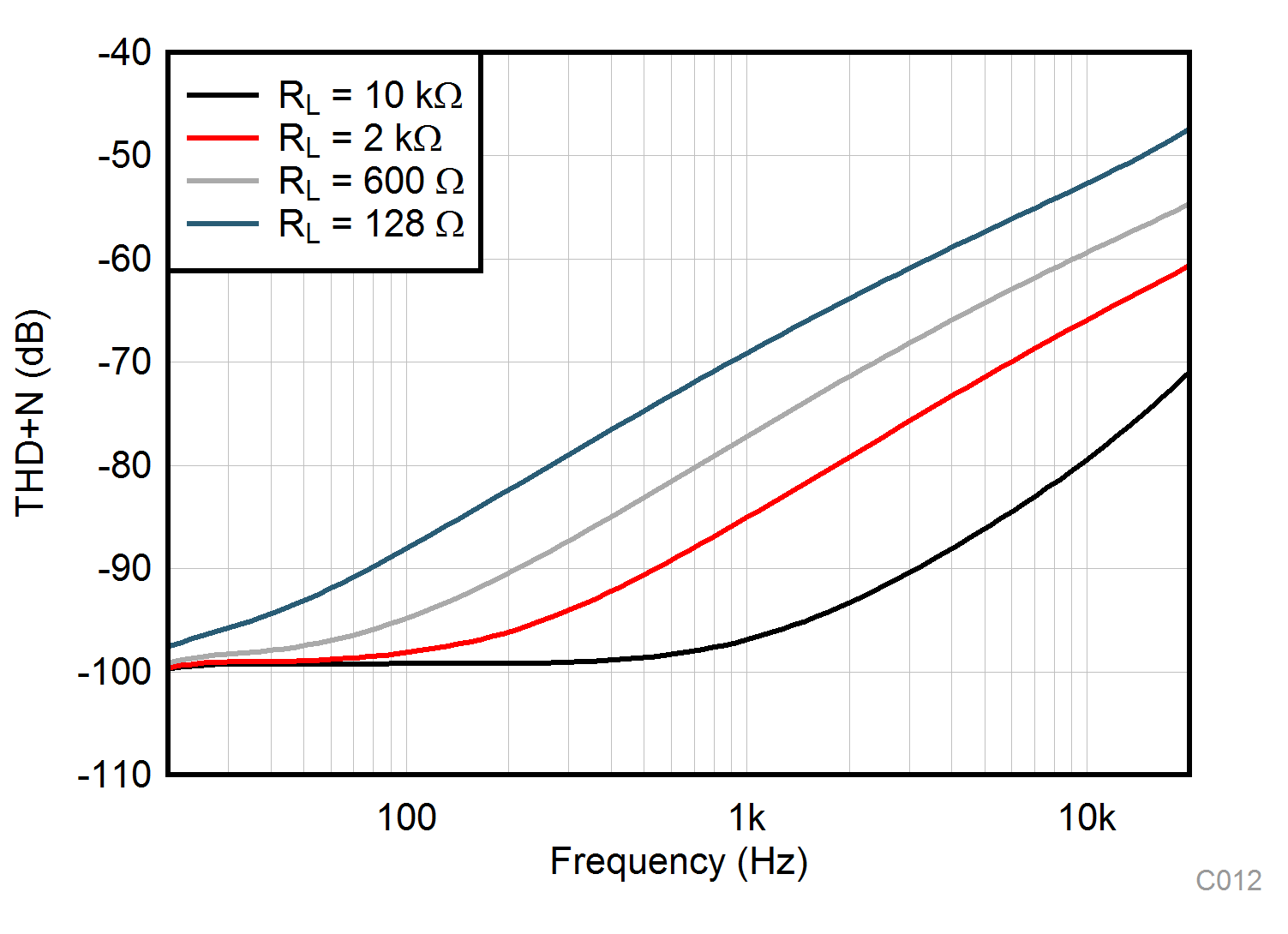
| BW = 80kHz,
VOUT = 3.5VRMS |
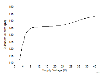 Figure 5-22 Quiescent
Current vs Supply Voltage
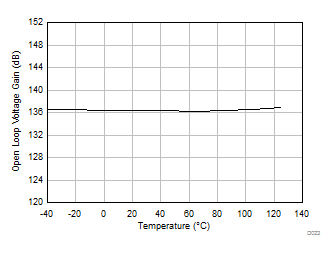 Figure 5-24 Open-Loop
Voltage Gain vs Temperature (dB)
| G = –1, 100mV output step |
| G = –1, 100mV output step |
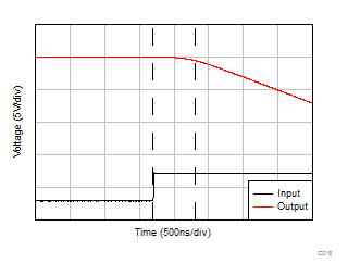 Figure 5-30 Positive
Overload Recovery
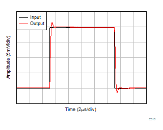
| CL =
20pF, G = 1, 20mV step response |
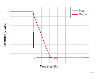 Figure 5-34 Large-Signal
Step Response (Falling)
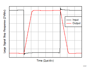 Figure 5-36 Large-Signal
Step Response
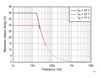 Figure 5-38 Maximum Output
Voltage vs Frequency
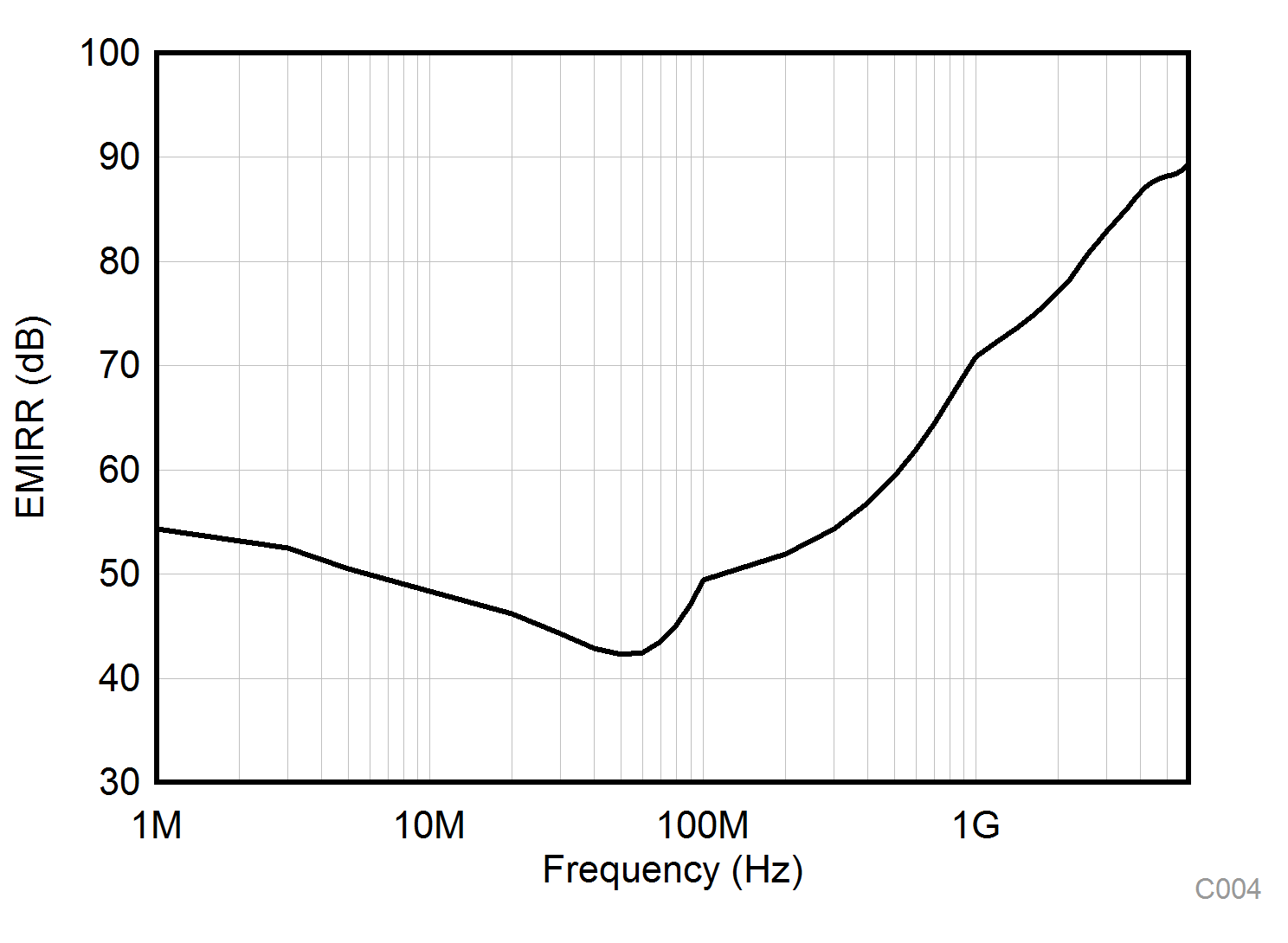 Figure 5-40 EMIRR
(Electromagnetic Interference Rejection Ratio) vs Frequency


 Figure 5-9 Input Bias
Current vs Common-Mode Voltage
 Figure 5-11 Output Voltage
Swing vs Output Current (Sourcing)


 Figure 5-23 Quiescent
Current vs Temperature


 Figure 5-39 Channel
Separation vs Frequency


 Figure 5-10 Input Bias
Current vs Temperature
 Figure 5-12 Output Voltage
Swing vs Output Current (Sinking)


 Figure 5-24 Open-Loop
Voltage Gain vs Temperature (dB)


 Figure 5-40 EMIRR
(Electromagnetic Interference Rejection Ratio) vs Frequency