SBOS994E November 2019 – January 2022 TLV9351 , TLV9352 , TLV9354
PRODUCTION DATA
- 1 Features
- 2 Applications
- 3 Description
- 4 Revision History
- 5 Pin Configuration and Functions
- 6 Specifications
- 7 Detailed Description
- 8 Application Information Disclaimer
- 9 Power Supply Recommendations
- 10Layout
- 11Device and Documentation Support
- 12Mechanical, Packaging, and Orderable Information
Package Options
Mechanical Data (Package|Pins)
Thermal pad, mechanical data (Package|Pins)
Orderable Information
7.3.5 Capacitive Load and Stability
The TLV935x features a resistive output stage capable of driving smaller capacitive loads, and by leveraging an isolation resistor, the device can easily be configured to drive large capacitive loads. Increasing the gain enhances the ability of the amplifier to drive greater capacitive loads; see Figure 7-5 and Figure 7-6. The particular op amp circuit configuration, layout, gain, and output loading are some of the factors to consider when establishing whether an amplifier is stable in operation.
 Figure 7-5 Small-Signal Overshoot vs Capacitive Load (100-mV Output Step, G = 1)
 Figure 7-6 Small-Signal Overshoot vs Capacitive Load (100-mV Output Step, G = –1)
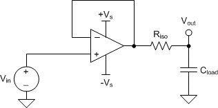
For additional drive capability in unity-gain configurations, improve capacitive load drive by inserting a small (10 Ω to 20 Ω) resistor, RISO, in series with the output, as shown in Figure 7-7. This resistor significantly reduces ringing and maintains DC performance for purely capacitive loads. However, if a resistive load is in parallel with the capacitive load, then a voltage divider is created, thus introducing a gain error at the output and slightly reducing the output swing. The error introduced is proportional to the ratio RISO / RL, and is generally negligible at low output levels. A high capacitive load drive makes the TLV935x well suited for applications such as reference buffers, MOSFET gate drives, and cable-shield drives. The circuit shown in Figure 7-7 uses an isolation resistor, RISO, to stabilize the output of an op amp. RISO modifies the open-loop gain of the system for increased phase margin. For additional information on techniques to optimize and design using this circuit, TI Precision Design TIDU032 details complete design goals, simulation, and test results.
 Figure 7-7 Extending Capacitive Load Drive With the TLV9351