SLYS029C July 2021 – December 2024 TMAG5110-Q1 , TMAG5111-Q1
PRODUCTION DATA
- 1
- 1 Features
- 2 Applications
- 3 Description
- 4 Device Comparison Table
- 5 Pin Configuration and Functions
- 6 Specifications
- 7 Detailed Description
- 8 Application and Implementation
- 9 Device and Documentation Support
- 10Revision History
- 11Mechanical, Packaging, and Orderable Information
Package Options
Refer to the PDF data sheet for device specific package drawings
Mechanical Data (Package|Pins)
- DBV|5
Thermal pad, mechanical data (Package|Pins)
Orderable Information
7.3.3 Power-On Time
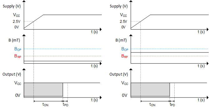
Figure 7-17 shows the behavior of the device after the VCC voltage is applied and when the field is below the BOP threshold. When the minimum value for VCC is reached, the TMAG5110-Q1 takes time tON to power up and then time tPD to update the output to a level High.
Figure 7-18 shows the behavior of the device after the VCC voltage is applied and when the field is above the BOP threshold. When the minimum value for VCC is reached, the TMAG5110-Q1 takes time tON to power up and then time tPD to update the output to a level High.
For the TMAG5111-Q1, the power-on behavior is similar, but OUT1 updates to Low during the tPD time. OUT2 updates to High during the tPD time. The output value following the power-on sequence then depends on the magnet placement, the sense of rotation, and the device variant.
 Figure 7-17 Power-On Time When
B<BOP
 Figure 7-18 Power-On Time When
B>BOP
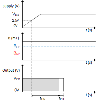
Figure 7-18 Power-On Time When
B>BOPTMAG5110-Q1 devices with the R pinout version have a Low output state during the tPD time. The output stays Low if the field sensed at power-on is between BOP and BRP, until BRP is crossed. This behavior for the TMAG5110-Q1 R pinout versions can be seen in Figure 7-19 and Figure 7-20.
 Figure 7-19 Power-On Time When
B<BOP (R Pinout Version)
 Figure 7-20 Power-On Time When
B>BOP (R Pinout Version)