SLYS033
November 2021
TMAG5124-Q1
PRODUCTION DATA
1
1
Features
2
Applications
3
Description
4
Revision History
5
Device Comparison
6
Pin Configuration and Functions
7
Specifications
7.1
Absolute Maximum Ratings
7.2
ESD Ratings
7.3
Recommended Operating Conditions
7.4
Thermal Information
7.5
Electrical Characteristics
7.6
Magnetic Characteristics
7.7
Typical Characteristics
7.7.1
TMAG5124A and TMAG5124E
7.7.2
TMAG5124B and TMAG5124F
7.7.3
TMAG5124C and TMAG5124G
7.7.4
TMAG5124D and TMAG5124H
7.7.5
Current Output Level
7.7.5.1
Low-Level Current Output for TMAG5124A/B/C/D
7.7.5.2
Low-Level Current Output for TMAG5124E/F/G/H
7.7.5.3
High-Level Current Output for Every Version
8
Detailed Description
8.1
Overview
8.2
Functional Block Diagram
8.3
Feature Description
8.3.1
Field Direction Definition
8.3.2
Device Output
8.3.3
Protection Circuits
8.3.3.1
Load Dump Protection
8.3.3.2
Reverse Polarity Protection
8.3.4
Power-On Time
8.3.5
Hall Element Location
8.3.6
Propagation Delay
8.3.7
Chopper Stabilization
8.4
Device Functional Modes
9
Application and Implementation
9.1
Application Information
9.2
Typical Applications
9.2.1
High-Side and Low-Side Typical Application Diagrams
9.2.1.1
Design Requirements
9.2.1.2
Detailed Design Procedure
9.2.1.3
Application Curve
10
Power Supply Recommendations
10.1
Power Derating
11
Layout
11.1
Layout Guidelines
11.2
Layout Example
12
Device and Documentation Support
12.1
Documentation Support
12.2
Receiving Notification of Documentation Updates
12.3
Support Resources
12.4
Trademarks
12.5
Electrostatic Discharge Caution
12.6
Glossary
13
Mechanical, Packaging, and Orderable Information
Package Options
Mechanical Data (Package|Pins)
DBZ|3
MPDS108G
Thermal pad, mechanical data (Package|Pins)
Orderable Information
slys033_oa
slys033_pm
7.7.2
TMAG5124B and TMAG5124F
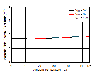
Figure 7-7
B
OP
vs. Temperature
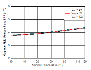
Figure 7-9
B
RP
vs. Temperature
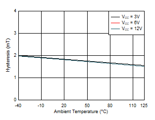
Figure 7-11
Hysteresis vs. Temperature
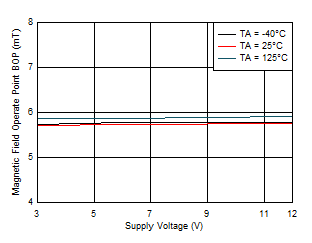
Figure 7-8
B
OP
vs. V
CC
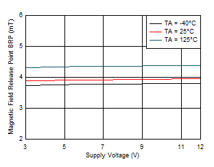
Figure 7-10
B
RP
vs. V
CC
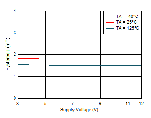
Figure 7-12
Hysteresis vs. V
CC