SLYS033 November 2021 TMAG5124-Q1
PRODUCTION DATA
- 1
- 1 Features
- 2 Applications
- 3 Description
- 4 Revision History
- 5 Device Comparison
- 6 Pin Configuration and Functions
-
7 Specifications
- 7.1 Absolute Maximum Ratings
- 7.2 ESD Ratings
- 7.3 Recommended Operating Conditions
- 7.4 Thermal Information
- 7.5 Electrical Characteristics
- 7.6 Magnetic Characteristics
- 7.7 Typical Characteristics
- 8 Detailed Description
- 9 Application and Implementation
- 10Power Supply Recommendations
- 11Layout
- 12Device and Documentation Support
- 13Mechanical, Packaging, and Orderable Information
Package Options
Mechanical Data (Package|Pins)
- DBZ|3
Thermal pad, mechanical data (Package|Pins)
Orderable Information
8.3.6 Propagation Delay
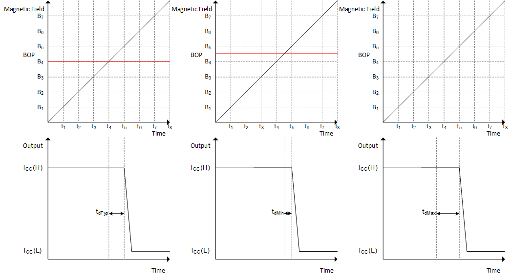
The TMAG5124-Q1 samples the Hall element at a nominal sampling interval of 12.5 µs to detect the presence of a magnetic south pole. Between each sampling interval, the device calculates the average magnetic field applied to the device. If this average value crosses the BOP or BRP threshold, the device changes the corresponding level as defined in Figure 8-3. The hall sensor + magnet system is by nature asynchronous, therefore the propagation delay (td) will vary depending on when the magnetic field goes above the BOP value. Figure 8-7 shows that the output delay also depends on when the magnetic field goes above the BOP value.
The first graph in Figure 8-7 shows the typical case. The magnetic field goes above the BOP value at the moment the output is updated. The part will only require one sampling period of 12.5 µs to update the output.
The second graph in Figure 8-7 shows a magnetic field going above the BOP value just before half of the sampling period. This is the best-case scenario where the output is updated in just half of the sampling period.
Finally, the third graph in Figure 8-7 shows the worst-case scenario where the magnetic field goes above the BOP value just after half of the sampling period. At the next output update, the device will still see the magnetic field under the BOP threshold and will require a whole new sampling period to update the output.
 Figure 8-7 Field Sampling Timing
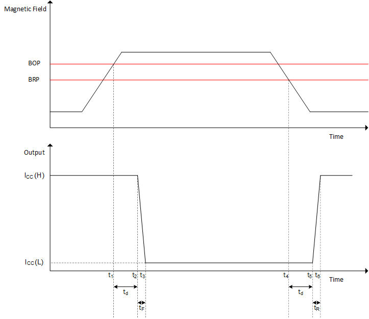
Figure 8-8 shows the TMAG5124-Q1 propagation delay analysis when a magnetic south pole is applied. The Hall element of the TMAG5124-Q1 experiences an increasing magnetic field as a magnetic south pole approaches the device, as well as a decreasing magnetic field as a magnetic south pole moves away. At time t1, the magnetic field goes above the BOP threshold. The output will then start to move after the propagation delay (td). This time will vary depending on when the sampling period is, as shown in Figure 8-7. At t2, the output start pulling to the low current value. At t3, the output is completely pulled down to the lower current value. The same process happens on the other way when the magnetic value is going under the BRP threshold.
 Figure 8-8 Propagation Delay